
EPF10K100EFC256-3N
| Part Description |
FLEX-10KE® Field Programmable Gate Array (FPGA) IC 191 49152 4992 256-BGA |
|---|---|
| Quantity | 1,684 Available (as of June 15, 2026) |

| Product Category | Field Programmable Gate Array (FPGA) |
|---|---|
| Manufacturer | Intel |
| Manufacturing Status | Obsolete |
| Manufacturer Standard Lead Time | Contact Us |
| Datasheet |
Specifications & Environmental
| Device Package | 256-FBGA (17x17) | Grade | Commercial | Operating Temperature | 0°C – 70°C | ||
|---|---|---|---|---|---|---|---|
| Package / Case | 256-BGA | Number of I/O | 191 | Voltage | 2.375 V - 2.625 V | ||
| Mounting Method | Surface Mount | RoHS Compliance | Unknown | REACH Compliance | REACH Unaffected | ||
| Moisture Sensitivity Level | 3 (168 Hours) | Number of LABs/CLBs | 624 | Number of Logic Elements/Cells | 4992 | ||
| Number of Gates | 257000 | ECCN | 3A001A2A | HTS Code | 8542.39.0001 | ||
| Qualification | N/A | Total RAM Bits | 49152 |
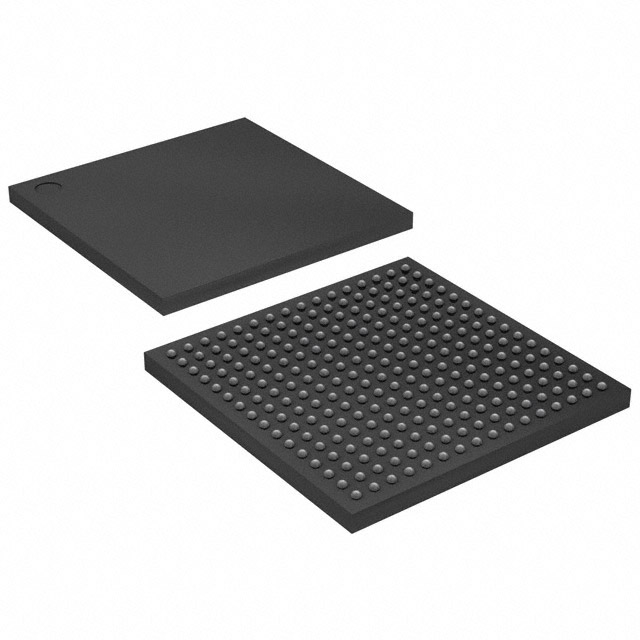
Overview of EPF10K100EFC256-3N – FLEX-10KE® Field Programmable Gate Array (FPGA) IC — 4992 logic elements, 191 I/Os, 256‑BGA
The EPF10K100EFC256-3N is a FLEX‑10KE family field programmable gate array from Intel, offered in a 256‑ball BGA package. It provides a mid‑density programmable logic platform with 4,992 logic elements, significant embedded RAM, and a broad I/O count suited for complex glue‑logic, protocol bridging, and embedded control tasks.
Designed for commercial applications, this surface‑mount FPGA balances on‑chip memory, I/O capacity, and reconfigurability to accelerate prototyping and production designs that require flexible hardware-based logic and system integration.
Key Features
- Programmable logic capacity — 4,992 logic elements supporting a device gate count of 257,000 for implementing custom logic, state machines, and datapath functions.
- Embedded memory — 49,152 total RAM bits of on‑chip memory to support FIFOs, small buffers, and state storage without external RAM.
- I/O and package — 191 user I/O pins delivered in a 256‑BGA (256‑FBGA, 17×17) package, optimized for high‑pin‑count board routing and dense system designs.
- Supply and mounting — Core supply range of 2.375 V to 2.625 V; supplied as a surface‑mount device for standard PCB assembly flows.
- Logic array blocks (LABs) — 624 LABs to organize logic into repeatable blocks and simplify place‑and‑route strategies.
- Commercial temperature grade — Specified for 0 °C to 70 °C operation, appropriate for general‑purpose embedded and electronic equipment.
- Family-level system features — Supports in‑circuit reconfigurability and IEEE‑1149.1 JTAG boundary‑scan for device programming and test access; includes architecture features such as dedicated carry and cascade chains and low‑skew clock distribution (family datasheet).
- RoHS compliant — Conforms to RoHS requirements for lead‑free assembly and environmental compliance.
Typical Applications
- Embedded control and automation — Implement custom control logic, interface decoders, and real‑time state machines using the device’s logic elements and embedded RAM.
- Protocol bridging and interface adaptation — Use the 191 I/O pins and programmable logic to bridge between disparate bus standards or to implement board‑level protocol converters.
- Prototyping and hardware acceleration — Rapidly prototype system functions and offload compute‑intensive tasks from microcontrollers or DSPs by mapping algorithms into programmable logic and on‑chip memory.
- Peripheral and I/O expansion — Add custom I/O timing, buffering, and glue logic to expand or adapt peripheral interfaces without redesigning host systems.
Unique Advantages
- Balanced resource mix: Combines nearly 5,000 logic elements with 49,152 bits of embedded RAM, allowing both control logic and small data structures to reside on‑chip and reducing external memory needs.
- High I/O density: 191 user I/Os in a 256‑BGA package support rich peripheral connectivity and board-level multiplexing without sacrificing package density.
- Reconfigurable hardware: In‑circuit reconfigurability and JTAG boundary‑scan enable design iteration, field updates, and board‑level testability without consuming user logic.
- Predictable timing building blocks: Dedicated carry and cascade chains and low‑skew clock distribution (family features) simplify implementation of arithmetic and high‑fan‑in logic, improving design predictability.
- Commercial readiness: Surface‑mount 256‑FBGA package and RoHS compliance align with standard assembly processes for production volumes.
Why Choose EPF10K100EFC256-3N?
The EPF10K100EFC256-3N positions itself as a versatile mid‑density FPGA for teams that need reprogrammable hardware with a balanced combination of logic, embedded memory, and a large I/O count. Its 256‑BGA package and surface‑mount format make it suitable for compact, production PCBs while the FLEX‑10K family system features—such as JTAG programming and architecture optimizations—help accelerate development and system integration.
This device is well suited for embedded designers and procurement teams targeting commercial applications that require flexible logic implementation, on‑chip buffering, and accessible I/O resources with the supply and temperature characteristics listed in the product specifications.
Request a quote or submit a parts inquiry to receive pricing and availability for EPF10K100EFC256-3N and to discuss how this FLEX‑10KE device can fit into your next design.


Date Founded: 1968
Headquarters: Santa Clara, California, USA
Employees: 130,000+
Revenue: $54.23 Billion
Certifications and Memberships: ISO9001:2015, ISO14001:2015, ISO17025:2017, ISO27001:2022, ISO45001:2018, ISO50001:2018


