
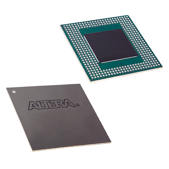
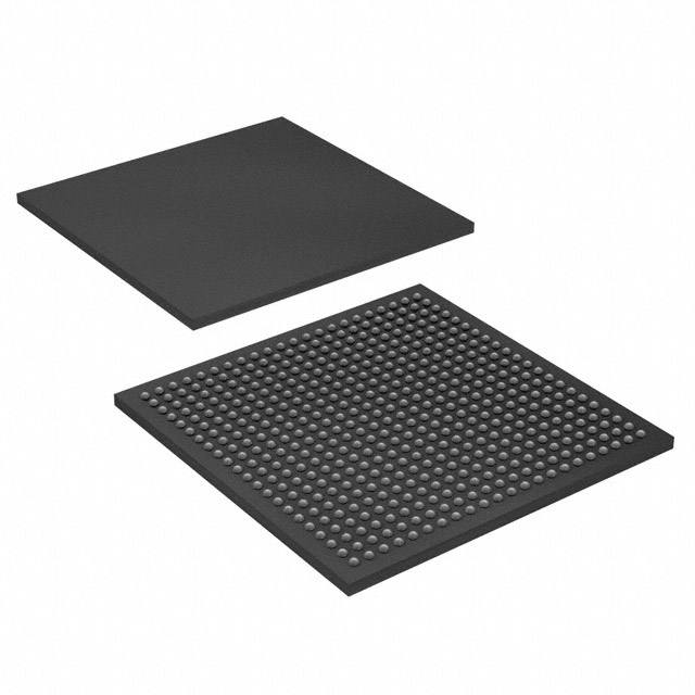
EPF10K200SFC484-1
| Part Description |
FLEX-10KS® Field Programmable Gate Array (FPGA) IC 369 98304 9984 484-BBGA |
|---|---|
| Quantity | 62 Available (as of June 18, 2026) |

| Product Category | Field Programmable Gate Array (FPGA) |
|---|---|
| Manufacturer | Intel |
| Manufacturing Status | Obsolete |
| Manufacturer Standard Lead Time | Contact Us |
| Datasheet |
Specifications & Environmental
| Device Package | 484-FBGA (23x23) | Grade | Commercial | Operating Temperature | 0°C – 70°C | ||
|---|---|---|---|---|---|---|---|
| Package / Case | 484-BBGA | Number of I/O | 369 | Voltage | 2.375 V - 2.625 V | ||
| Mounting Method | Surface Mount | RoHS Compliance | Unknown | REACH Compliance | REACH Unaffected | ||
| Moisture Sensitivity Level | 3 (168 Hours) | Number of LABs/CLBs | 1248 | Number of Logic Elements/Cells | 9984 | ||
| Number of Gates | 513000 | ECCN | 3A001A2A | HTS Code | 8542.39.0001 | ||
| Qualification | N/A | Total RAM Bits | 98304 |
Overview of EPF10K200SFC484-1 – FLEX-10KS Field Programmable Gate Array, 9,984 logic elements, 369 I/O
The EPF10K200SFC484-1 is an Intel FLEX 10K series embedded programmable logic device designed for configurable system integration. It combines a high-density logic array with substantial on-chip RAM and a large I/O count to address mid-range FPGA requirements.
As a member of the FLEX 10K family, this device targets system-level integration use cases—implementing custom logic, memory-intensive functions, and flexible I/O interfacing—while providing features that support in-circuit reconfigurability and boundary-scan testability.
Key Features
- Logic Capacity Approximately 9,984 logic elements implemented across 1,248 LABs, enabling complex combinational and sequential logic designs.
- Embedded Memory Total on-chip RAM of 98,304 bits (approximately 0.098 Mbits) for storage of lookup tables, FIFOs, and small buffers without external memory.
- I/O and Interconnect 369 user I/O pins for rich peripheral and bus interfacing; the FLEX 10K family provides flexible I/O options and dedicated interconnect resources.
- Gate Count Device-level gate equivalent of 513,000, reflecting overall logic and routing resources available to the design.
- In-Circuit Reconfigurability & Test Supports in-circuit reconfiguration and includes built-in JTAG boundary-scan test circuitry compliant with IEEE Std. 1149.1 for board-level test and debug.
- Power Supply Operates from a defined core voltage range of 2.375 V to 2.625 V.
- Package & Mounting 484-ball BGA in a 23 × 23 footprint (supplier package: 484-FBGA), surface-mount package for compact board integration.
- Operating Conditions & Compliance Commercial grade with an operating temperature range of 0 °C to 70 °C and RoHS compliance.
Typical Applications
- Embedded Systems Implement custom logic blocks, protocol bridges, and on-chip memory buffering for embedded controller and appliance designs.
- Control & Signal Processing Use the device’s logic density and embedded RAM to implement data-path functions, finite-state machines, and moderate DSP tasks.
- Prototyping & Development Rapidly iterate hardware designs and verify system-level integration with in-circuit reconfigurability and JTAG boundary-scan support.
- Interface Concentration Aggregate multiple peripheral interfaces and custom I/O functions using a high I/O count and flexible interconnect resources.
Unique Advantages
- Balanced Logic and Memory Nearly 10k logic elements combined with 98,304 bits of embedded RAM lets you implement logic-intensive functions alongside on-chip storage without immediate reliance on external memory.
- High I/O Density 369 I/O pins give designers the flexibility to connect multiple peripherals, buses, or sensors directly to the FPGA fabric.
- Board-Level Testability Built-in IEEE 1149.1 JTAG boundary-scan simplifies manufacturing test and in-system debug.
- Compact, Surface-Mount Packaging 484-ball BGA (23×23) package enables a high-pin-count solution in a space-efficient footprint suitable for dense PCBs.
- Commercial Operating Range Commercial-grade specification with defined 0 °C to 70 °C operation and RoHS compliance for mainstream electronic products.
Why Choose EPF10K200SFC484-1?
The EPF10K200SFC484-1 provides a balanced combination of logic density, embedded RAM, and I/O capacity suited to mid-range FPGA use cases where on-chip memory and flexible interfacing are important. Its FLEX 10K family heritage brings system-level capabilities including in-circuit reconfiguration and boundary-scan testability that help accelerate development and production testing.
This device is appropriate for designers building embedded systems, interface concentrators, or prototype platforms that require a compact BGA package, a defined commercial temperature range, and RoHS compliance. Its specific mix of logic elements, LABs, and RAM supports scalable designs within the FLEX 10K architecture.
Request a quote or submit an RFQ to obtain pricing and availability for the EPF10K200SFC484-1 and to discuss how this device fits your next design.


Date Founded: 1968
Headquarters: Santa Clara, California, USA
Employees: 130,000+
Revenue: $54.23 Billion
Certifications and Memberships: ISO9001:2015, ISO14001:2015, ISO17025:2017, ISO27001:2022, ISO45001:2018, ISO50001:2018


