
EPF10K30AFC256-3
| Part Description |
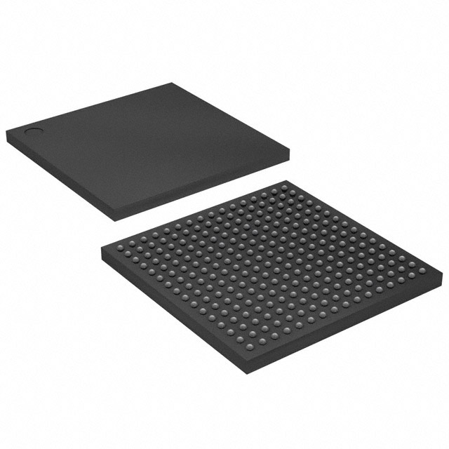
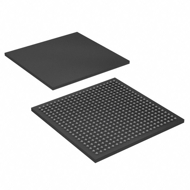
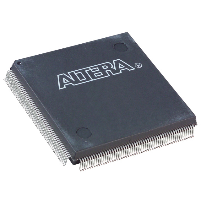
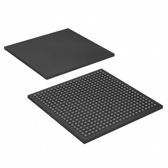
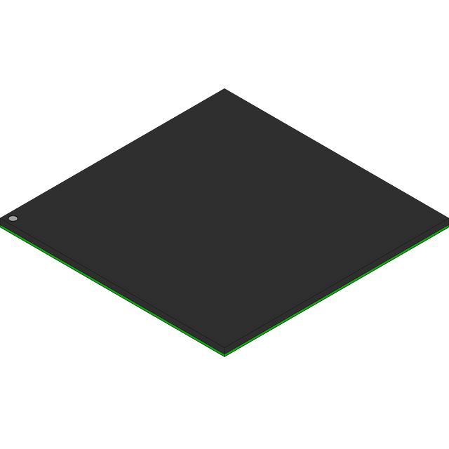
FLEX-10KA® Field Programmable Gate Array (FPGA) IC 191 12288 1728 256-BGA |
|---|---|
| Quantity | 717 Available (as of October 8, 2026) |
| Product Category | Field Programmable Gate Array (FPGA) |
|---|---|
| Manufacturer | Intel |
| Manufacturing Status | Obsolete |
| Manufacturer Standard Lead Time | Contact Us |
| Datasheet |
Specifications & Environmental
| Device Package | 256-FBGA (17x17) | Grade | Commercial | Operating Temperature | 0°C – 70°C | ||
|---|---|---|---|---|---|---|---|
| Package / Case | 256-BGA | Number of I/O | 191 | Voltage | 3 V - 3.6 V | ||
| Mounting Method | Surface Mount | RoHS Compliance | Unknown | REACH Compliance | REACH Unaffected | ||
| Moisture Sensitivity Level | 3 (168 Hours) | Number of LABs/CLBs | 216 | Number of Logic Elements/Cells | 1728 | ||
| Number of Gates | 69000 | ECCN | 3A001A2A | HTS Code | 8542.39.0001 | ||
| Qualification | N/A | Total RAM Bits | 12288 |
Overview of EPF10K30AFC256-3 – FLEX-10KA Field Programmable Gate Array (FPGA), 256-BGA
The EPF10K30AFC256-3 is a FLEX-10KA family field programmable gate array (FPGA) in a 256-ball fine-pitch BGA package. It combines a programmable logic array and embedded memory resources to support system-on-a-programmable-chip (SOPC) integration and megafunction implementation.
Designed for commercial embedded designs, this device provides mid-range logic and memory capacity with a broad I/O count and a compact 256-FBGA (17×17) footprint, supporting 3.0 V to 3.6 V supply operation and a 0 °C to 70 °C operating range.
Key Features
- Core Logic Approximately 1,728 logic elements implemented across 216 logic array blocks (LABs), supporting a typical system gate count of up to 69,000 gates.
- Embedded Memory 12,288 total RAM bits of embedded on-chip RAM suitable for implementing megafunctions and local buffering.
- I/O and Interfaces Up to 191 user I/O pins for flexible peripheral interfacing and board-level connectivity.
- Package 256-ball Fine-Pitch BGA (256-FBGA, 17×17) surface-mount package for high-density board integration.
- Power and Temperature Operates from 3.0 V to 3.6 V with a commercial operating temperature range of 0 °C to 70 °C.
- System Integration Family-level features include embedded arrays for megafunctions, in-circuit reconfigurability options via external configuration device or JTAG, and built-in JTAG boundary-scan test circuitry.
- Performance and Routing Family architecture provides dedicated carry and cascade chains and a continuous routing structure for predictable interconnect delays.
- Compliance and Testability RoHS-compliant device with built-in IEEE 1149.1 JTAG boundary-scan support for board-level test and configuration.
Typical Applications
- Embedded Systems Implement SOPC building blocks and custom logic in compact embedded controllers where moderate logic density and embedded RAM are required.
- Peripheral and Interface Glue Logic Use the device’s 191 I/O pins and flexible I/O control to implement bus bridging, protocol conversion, and board-level interface logic.
- Memory-Backed Megafunctions Deploy the embedded RAM for FIFOs, small buffers, and other memory-backed functions integrated with custom logic.
- Prototyping and Evaluation Mid-range gate density and a fine-pitch BGA package make the part suitable for hardware prototyping and functional evaluation of system-level designs.
Unique Advantages
- Balanced Logic and Memory: 1,728 logic elements paired with 12,288 RAM bits deliver a practical mix of resources for mid-range FPGA tasks without over-provisioning.
- High I/O Count in a Compact Package: 191 I/O pins in a 256-FBGA (17×17) package reduce board area while preserving connectivity for peripherals and interfaces.
- System-Level Integration: Embedded array support for megafunctions and JTAG-based in-circuit reconfiguration simplify integration of common system functions and testing.
- Deterministic Routing and Arithmetic Support: Dedicated carry and cascade chains and a continuous interconnect structure help achieve predictable timing for arithmetic and high-fan-in logic.
- Commercial Temperature and Voltage Compatibility: Specified for 3.0 V–3.6 V operation and 0 °C–70 °C ambient, suitable for a wide range of commercial applications.
- Manufacturing and Test-Ready: Built-in JTAG boundary-scan and RoHS compliance aid board-level testability and manufacturing acceptance.
Why Choose EPF10K30AFC256-3?
The EPF10K30AFC256-3 occupies a practical middle ground for designs that need a balanced combination of logic elements, embedded RAM, and I/O without moving to larger, more complex devices. Its FLEX-10KA family architecture supports system-level megafunctions and in-circuit reconfiguration options, enabling designers to integrate memory and specialized logic alongside general-purpose programmable resources.
This device is well suited for commercial embedded designs, interface logic, and prototype systems where compact packaging, testability, and predictable routing are important. The combination of 1,728 logic elements, 12,288 RAM bits, 191 I/Os, and a 256-FBGA package provides a scalable option within the FLEX 10K family for projects that require measurable integration and flexibility.
Request a quote or submit an inquiry to evaluate EPF10K30AFC256-3 for your next design project.






















Date Founded: 1968
Headquarters: Santa Clara, California, USA
Employees: 130,000+
Revenue: $54.23 Billion
Certifications and Memberships: ISO9001:2015, ISO14001:2015, ISO17025:2017, ISO27001:2022, ISO45001:2018, ISO50001:2018


