
EPF10K30AQC208-1N
| Part Description |
FLEX-10KA® Field Programmable Gate Array (FPGA) IC 147 12288 1728 208-BFQFP |
|---|---|
| Quantity | 41 Available (as of June 15, 2026) |

| Product Category | Field Programmable Gate Array (FPGA) |
|---|---|
| Manufacturer | Intel |
| Manufacturing Status | Obsolete |
| Manufacturer Standard Lead Time | Contact Us |
| Datasheet |
Specifications & Environmental
| Device Package | 208-PQFP (28x28) | Grade | Commercial | Operating Temperature | 0°C – 70°C | ||
|---|---|---|---|---|---|---|---|
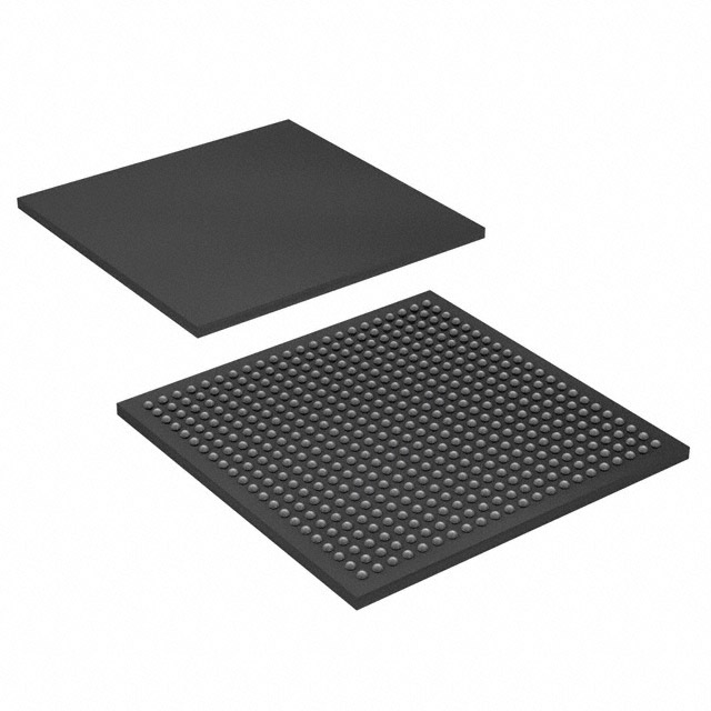
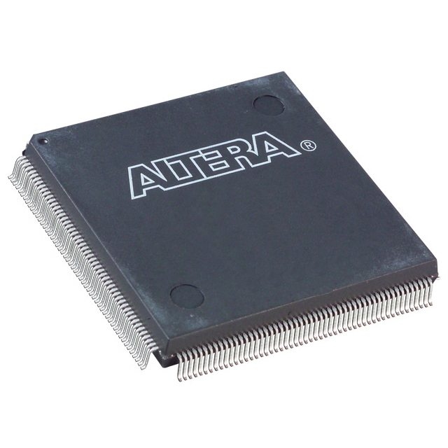
| Package / Case | 208-BFQFP | Number of I/O | 147 | Voltage | 3 V - 3.6 V | ||
| Mounting Method | Surface Mount | RoHS Compliance | Unknown | REACH Compliance | REACH Unaffected | ||
| Moisture Sensitivity Level | 3 (168 Hours) | Number of LABs/CLBs | 216 | Number of Logic Elements/Cells | 1728 | ||
| Number of Gates | 69000 | ECCN | 3A001A2A | HTS Code | 8542.39.0001 | ||
| Qualification | N/A | Total RAM Bits | 12288 |
Overview of EPF10K30AQC208-1N – FLEX-10KA Field Programmable Gate Array (FPGA) IC, 208-BFQFP
The EPF10K30AQC208-1N is a FLEX 10KA family field programmable gate array (FPGA) in a 208-pin BFQFP package. It combines a logic array and embedded array blocks to implement general logic and memory-intensive megafunctions for commercial electronic designs.
Designed for mid-range integration, the device provides 1,728 logic elements, 12,288 bits of embedded RAM, and up to 147 user I/O pins while operating from a 3.0 V to 3.6 V supply at a commercial grade operating range of 0 °C to 70 °C.
Key Features
- Core Architecture FLEX 10KA family architecture with 1,728 logic elements and 216 logic array blocks (LABs) for implementing combinational and sequential logic.
- Embedded Memory 12,288 total RAM bits of embedded memory suitable for on-chip buffers and small data structures.
- I/O and Voltage 147 user I/O pins with MultiVolt I/O support; device operates from 3.0 V to 3.6 V and FLEX 10KA devices include 5.0-V tolerant input capability as documented for the family.
- Programmability and Test In-circuit reconfigurability via external configuration device, intelligent controller, or JTAG port; includes JTAG boundary-scan circuitry compliant with IEEE Std. 1149.1-1990.
- Clock and Timing Built-in low-skew clock distribution trees with ClockLock and ClockBoost options (family features) and support for multiple global clock and clear signals.
- Dedicated Arithmetic and Logic Chains Dedicated carry and cascade chains in the fabric to implement adders, counters, comparators, and high-fan-in logic functions efficiently.
- I/O Control Options Per-pin tri-state output enable, open-drain option, and programmable output slew-rate control to help manage interface behavior and switching noise.
- Package and Mounting 208-BFQFP (208-PQFP, 28 × 28 mm outline) surface-mount package for high-density PCB integration; RoHS compliant.
- Power and Grade Commercial grade device with typical low-power standby behavior reported for the family; supply range of 3.0 V–3.6 V.
Typical Applications
- System Integration / SOPC System-on-a-Programmable-Chip (SOPC) integration and glue logic where embedded memory and reconfigurable logic simplify board-level design.
- Interface and Bus Bridging Custom peripheral or bus interface logic, including PCI-compatible implementations supported by the FLEX 10K family.
- Embedded Control and Glue Logic Control functions, protocol handling, and timing-critical logic that benefit from dedicated carry/cascade chains and low-skew clock distribution.
- Memory-Dependent Logic Functions requiring on-chip buffers or small embedded storage using the device’s 12,288 bits of RAM.
Unique Advantages
- Balanced Integration: Combines 1,728 logic elements with 12,288 bits of embedded RAM to implement both logic and memory functions on a single device, reducing external component count.
- Flexible I/O Support: MultiVolt I/O and family support for 5.0-V tolerant inputs enable interfacing across common commercial voltage domains.
- Reconfigurability and Testability: In-circuit reconfigurability and IEEE 1149.1-compliant JTAG boundary-scan simplify configuration, debug, and production test flows.
- Deterministic Timing Resources: Low-skew clock trees, ClockLock/ClockBoost options, and dedicated arithmetic chains assist in meeting timing for performance-sensitive logic.
- Compact Surface-Mount Package: 208-BFQFP (28 × 28 mm) package provides a high pin-count solution in a surface-mount form factor suitable for dense boards.
- Regulatory Compliance: RoHS-compliant construction supports modern manufacturing and environmental requirements.
Why Choose EPF10K30AQC208-1N?
The EPF10K30AQC208-1N offers a mid-range FLEX 10KA FPGA option for designers who need a combination of reconfigurable logic, embedded RAM, and substantial I/O in a commercial-grade, surface-mount package. Its family-level features—such as MultiVolt I/O, JTAG boundary-scan, embedded array blocks, and dedicated arithmetic chains—make it suitable for a wide range of commercial electronic designs requiring on-chip memory and flexible interfacing.
This device is well suited to teams developing system integration logic, custom interfaces, and memory-backed control functions where compact packaging, reprogrammability, and adherence to common supply and temperature ranges (3.0 V–3.6 V, 0 °C–70 °C) are important for product delivery and lifecycle support.
If you would like pricing, availability, or to request a quote for EPF10K30AQC208-1N, submit a quote request or inquiry and our team will respond with details to support your purchasing and integration planning.


Date Founded: 1968
Headquarters: Santa Clara, California, USA
Employees: 130,000+
Revenue: $54.23 Billion
Certifications and Memberships: ISO9001:2015, ISO14001:2015, ISO17025:2017, ISO27001:2022, ISO45001:2018, ISO50001:2018


