
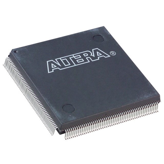
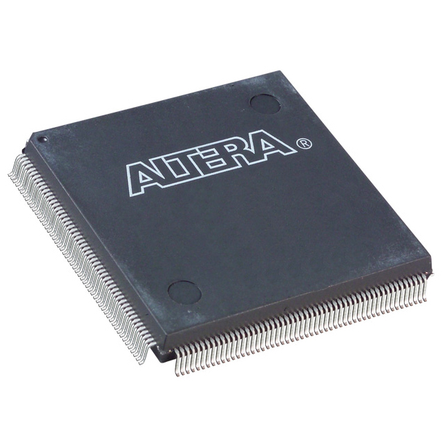
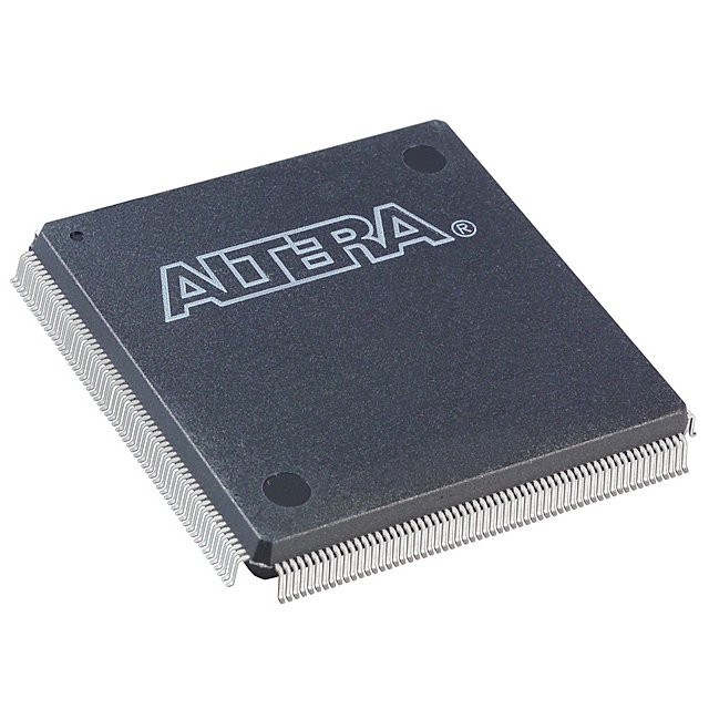
EPF10K30AQC208-3
| Part Description |
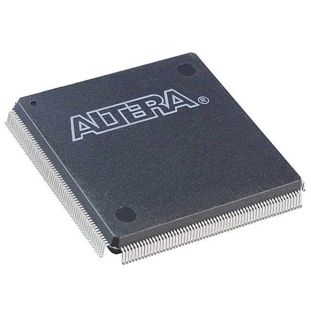
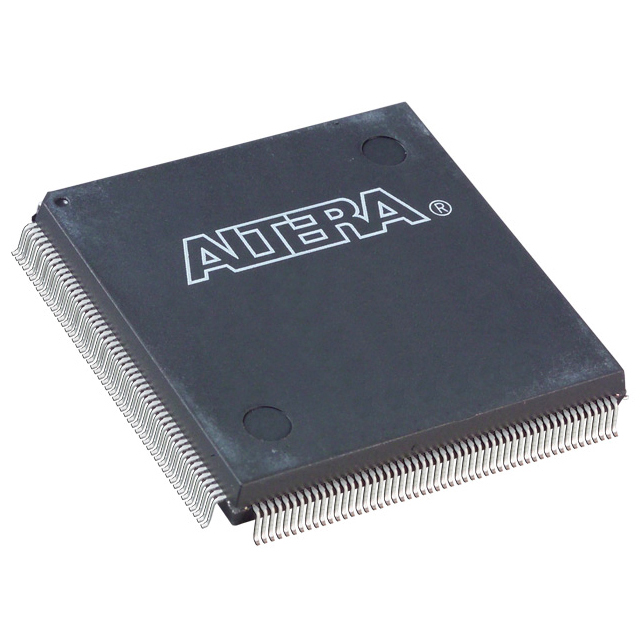
FLEX-10KA® Field Programmable Gate Array (FPGA) IC 147 12288 1728 208-BFQFP |
|---|---|
| Quantity | 769 Available (as of October 7, 2026) |
| Product Category | Field Programmable Gate Array (FPGA) |
|---|---|
| Manufacturer | Intel |
| Manufacturing Status | Obsolete |
| Manufacturer Standard Lead Time | Contact Us |
| Datasheet |
Specifications & Environmental
| Device Package | 208-PQFP (28x28) | Grade | Commercial | Operating Temperature | 0°C – 70°C | ||
|---|---|---|---|---|---|---|---|
| Package / Case | 208-BFQFP | Number of I/O | 147 | Voltage | 3 V - 3.6 V | ||
| Mounting Method | Surface Mount | RoHS Compliance | RoHS non-compliant | REACH Compliance | REACH Unaffected | ||
| Moisture Sensitivity Level | 3 (168 Hours) | Number of LABs/CLBs | 216 | Number of Logic Elements/Cells | 1728 | ||
| Number of Gates | 69000 | ECCN | 3A991D | HTS Code | 8542.39.0001 | ||
| Qualification | N/A | Total RAM Bits | 12288 |
Overview of EPF10K30AQC208-3 – FLEX-10KA® Field Programmable Gate Array (FPGA) IC 147 12288 1728 208-BFQFP
The EPF10K30AQC208-3 is a FLEX 10KA family field programmable gate array (FPGA) device providing embedded programmable logic for system-level integration. It combines a logic array and embedded memory resources to implement general logic functions and megafunctions for embedded system designs.
Designed for commercial-grade applications, the device targets embedded systems and board-level designs that require on-chip memory, flexible I/O, and in‑circuit reconfigurability within a 208-pin surface-mount package.
Key Features
- Logic Capacity Provides 1,728 logic elements and 216 logic array blocks for implementing combinational and sequential logic.
- Embedded Memory Approximately 12,288 bits of embedded RAM to support on-chip storage and megafunction memory blocks.
- I/O and Interfacing 147 user I/O pins with flexible I/O options; FLEX 10KA family supports MultiVolt I/O and 5.0‑V tolerant input pins as a family feature.
- Gate Density Documented device gate count: 69,000 gates (system gate metric included in product data).
- Power and Voltage Operates from 3.0 V to 3.6 V supply range compatible with 3.3 V systems; family-level features include low-power standby (typical <0.5 mA for most devices).
- Configuration and Test Supports in‑circuit reconfigurability via external configuration device or JTAG; includes JTAG boundary-scan test circuitry compliant with IEEE Std. 1149.1.
- Clocking and Arithmetic Support Family features include dedicated carry and cascade chains for efficient arithmetic and high‑fan‑in functions, plus low‑skew clock distribution.
- Package and Mounting 208‑BFQFP (208‑PQFP, 28×28) surface-mount package; supplier device package listed as 208‑PQFP (28×28).
- Operating Conditions Commercial grade operation from 0 °C to 70 °C and RoHS compliant.
Typical Applications
- Embedded System Integration On‑chip logic and embedded RAM enable consolidation of glue logic, controllers, and custom functions for compact system designs.
- Peripheral and Bus Interfaces Flexible I/O and family-level PCI support make the device suitable for implementing bus bridges and peripheral interface logic.
- Memory and Megafunction Implementation Embedded RAM blocks support on‑device FIFO, buffer, and small memory megafunctions to reduce external memory dependence.
- Prototyping and Custom Logic Reconfigurability and JTAG support facilitate board-level prototyping and iterative logic development.
Unique Advantages
- System-on-a-Programmable-Chip Integration: Embedded arrays and logic array combine to implement both specialized memory megafunctions and general logic on a single device, reducing BOM counts.
- Balanced Logic and Memory: 1,728 logic elements paired with ~12,288 bits of embedded RAM provide a balance of logic density and on‑chip storage for mixed workload designs.
- Flexible I/O: MultiVolt I/O support and 5.0‑V tolerant input capability (FLEX 10KA family feature) enable interfacing with a variety of board-level signaling standards.
- In‑Circuit Reconfigurability and Test: JTAG boundary-scan and in‑circuit reconfiguration options streamline programming, debug, and production test flow.
- Commercial Package and Compliance: 208‑pin surface-mount BFQFP package and RoHS compliance support standard assembly and regulatory expectations for commercial products.
- Clock and Arithmetic Optimizations: Dedicated carry and cascade chains and low‑skew clock trees help simplify implementation of high-speed adders, counters, and wide combinational logic.
Why Choose EPF10K30AQC208-3?
The EPF10K30AQC208-3 delivers a practical combination of logic resources, embedded memory, and flexible I/O in a commercial-grade, 208‑pin surface-mount package. Its family-level features—embedded programmable arrays, MultiVolt I/O, in‑circuit reconfiguration, and JTAG—support system integration tasks where consolidating functionality on-chip reduces board complexity.
This device is suited for designers developing embedded systems, peripheral interfaces, and prototyping platforms that require deterministic on‑chip memory, reconfigurable logic, and standard commercial operating conditions. Its RoHS compliance and common package format make it straightforward to integrate into existing production flows.
If you would like pricing, availability, or a formal quote for EPF10K30AQC208-3, submit an inquiry or request a quote through your procurement process.





















Date Founded: 1968
Headquarters: Santa Clara, California, USA
Employees: 130,000+
Revenue: $54.23 Billion
Certifications and Memberships: ISO9001:2015, ISO14001:2015, ISO17025:2017, ISO27001:2022, ISO45001:2018, ISO50001:2018


