
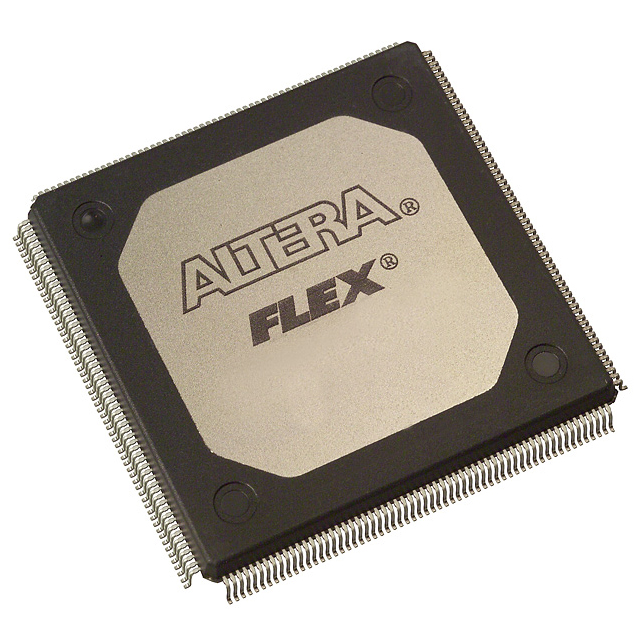
EPF10K50EFC256-2N
| Part Description |
FLEX-10KE® Field Programmable Gate Array (FPGA) IC 191 40960 2880 256-BGA |
|---|---|
| Quantity | 406 Available (as of June 15, 2026) |

| Product Category | Field Programmable Gate Array (FPGA) |
|---|---|
| Manufacturer | Intel |
| Manufacturing Status | Obsolete |
| Manufacturer Standard Lead Time | Contact Us |
| Datasheet |
Specifications & Environmental
| Device Package | 256-FBGA (17x17) | Grade | Commercial | Operating Temperature | 0°C – 70°C | ||
|---|---|---|---|---|---|---|---|
| Package / Case | 256-BGA | Number of I/O | 191 | Voltage | 2.3 V - 2.7 V | ||
| Mounting Method | Surface Mount | RoHS Compliance | Unknown | REACH Compliance | REACH Unaffected | ||
| Moisture Sensitivity Level | 3 (168 Hours) | Number of LABs/CLBs | 360 | Number of Logic Elements/Cells | 2880 | ||
| Number of Gates | 199000 | ECCN | 3A001A2A | HTS Code | 8542.39.0001 | ||
| Qualification | N/A | Total RAM Bits | 40960 |
Overview of EPF10K50EFC256-2N – FLEX-10KE® Field Programmable Gate Array (FPGA) IC 191 40960 2880 256-BGA
The EPF10K50EFC256-2N is a FLEX-10KE family FPGA from Intel designed for commercial embedded logic applications. It integrates 2,880 logic elements and on-chip memory to support complex combinational and sequential logic, enabling system-level functions and megafunction implementation.
This surface-mount FPGA is optimized for compact board designs with a 256-ball BGA package and 191 user I/O pins, making it suitable for commercial embedded systems, interface bridging, and logic acceleration tasks where reconfigurability and dense integration are required.
Key Features
- Logic Capacity — 2,880 logic elements and 199,000 gates provide substantial programmable logic resources for mid-density designs.
- Embedded Memory — 40,960 total RAM bits of embedded memory enable storage for FIFOs, buffers, and small on-chip data structures.
- I/O and Connectivity — 191 user I/O pins support a wide range of external interfaces and signal routing in a compact footprint.
- Power Supply — Designed for operation from 2.3 V to 2.7 V, providing defined supply requirements for system power design.
- Packaging — 256-BGA / 256-FBGA (17×17) package for high-density board integration and reliable solder mounting.
- Commercial Temperature Grade — Rated for operation from 0 °C to 70 °C for commercial applications.
- Board-Level Test and Reconfiguration — Supports JTAG boundary-scan (IEEE Std. 1149.1) and in-circuit reconfigurability via external configuration devices or intelligent controllers, aiding manufacturing test and field updates.
- Clock and Routing Features — Family-level features include low-skew clock distribution and clock management options for predictable timing and reduced clock skew.
- Surface Mount — Component is specified for surface-mount assembly to support modern PCB manufacturing processes.
- RoHS Compliant — Conforms to RoHS environmental requirements.
Typical Applications
- Embedded Control and Logic — Implement custom state machines, protocol handlers, and control logic using available logic elements and on-chip memory.
- Interface Bridging — Act as a programmable interface between subsystems where 191 I/O pins enable flexible signal routing and protocol adaptation.
- System Integration (SOPC) — Integrate specialized logic and memory megafunctions for compact system-on-programmable-chip solutions.
- Prototyping and Development — Use the reprogrammable nature and JTAG support for iterative design validation and in-circuit updates.
Unique Advantages
- Mid-density integration: 2,880 logic elements and 199,000 gates provide a balance of logic capacity without the footprint of larger devices.
- Embedded memory resources: 40,960 bits of on-chip RAM reduce dependence on external memory for many control and buffering tasks.
- Flexible I/O count: 191 user I/O pins give designers broad signal access for mixed-signal and multi-protocol designs.
- Testability and field serviceability: JTAG boundary-scan and in-circuit reconfiguration streamline manufacturing test and enable updates after deployment.
- Compact package: 256-FBGA (17×17) packaging supports high-density PCB layouts while maintaining robust solderability.
- Commercial-grade reliability: Rated for 0 °C to 70 °C operation and RoHS compliance for mainstream commercial applications.
Why Choose EPF10K50EFC256-2N?
The EPF10K50EFC256-2N positions itself as a flexible, mid-density FPGA option within Intel’s FLEX 10K family, combining programmable logic, embedded memory, and comprehensive I/O in a compact BGA package. Its mix of logic elements, on-chip RAM, and board-level test capabilities make it well suited for commercial embedded systems that require reconfigurability and modest capacity.
This device is appropriate for designers seeking a commercially rated programmable device with on-chip resources and established family-level features for clocking, routing, and JTAG-based test and configuration.
Request a quote or submit a procurement inquiry to begin evaluating EPF10K50EFC256-2N for your next embedded design project.


Date Founded: 1968
Headquarters: Santa Clara, California, USA
Employees: 130,000+
Revenue: $54.23 Billion
Certifications and Memberships: ISO9001:2015, ISO14001:2015, ISO17025:2017, ISO27001:2022, ISO45001:2018, ISO50001:2018


