
EPF10K50SFC256-3
| Part Description |
FLEX-10KS® Field Programmable Gate Array (FPGA) IC 191 40960 2880 256-BGA |
|---|---|
| Quantity | 1,571 Available (as of June 15, 2026) |

| Product Category | Field Programmable Gate Array (FPGA) |
|---|---|
| Manufacturer | Intel |
| Manufacturing Status | Obsolete |
| Manufacturer Standard Lead Time | Contact Us |
| Datasheet |
Specifications & Environmental
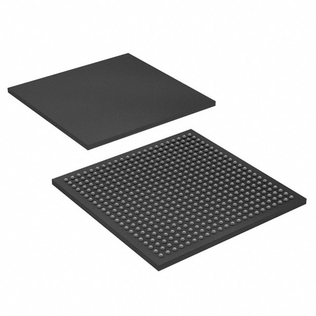
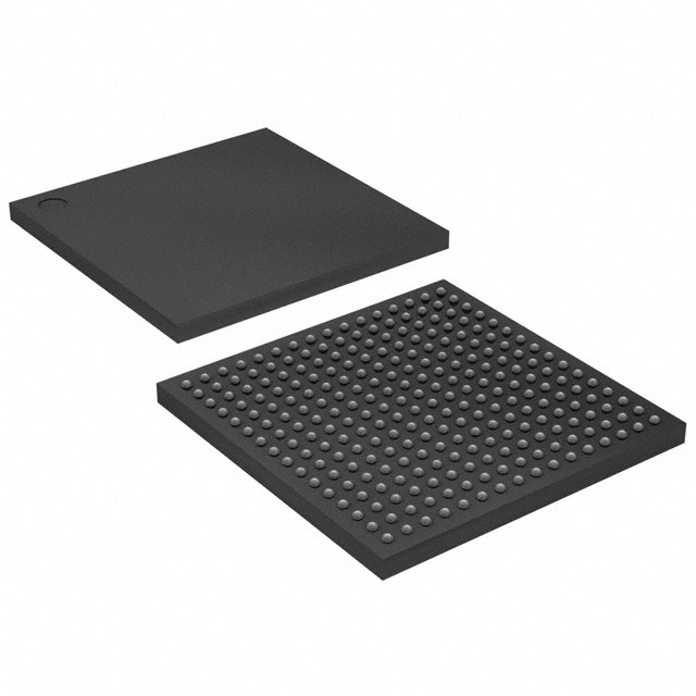
| Device Package | 256-FBGA (17x17) | Grade | Commercial | Operating Temperature | 0°C – 70°C | ||
|---|---|---|---|---|---|---|---|
| Package / Case | 256-BGA | Number of I/O | 191 | Voltage | 2.375 V - 2.625 V | ||
| Mounting Method | Surface Mount | RoHS Compliance | Unknown | REACH Compliance | REACH Unaffected | ||
| Moisture Sensitivity Level | 3 (168 Hours) | Number of LABs/CLBs | 360 | Number of Logic Elements/Cells | 2880 | ||
| Number of Gates | 199000 | ECCN | 3A001A2A | HTS Code | 8542.39.0001 | ||
| Qualification | N/A | Total RAM Bits | 40960 |
Overview of EPF10K50SFC256-3 – FLEX-10KS® Field Programmable Gate Array (FPGA), 256‑BGA
The EPF10K50SFC256-3 is a FLEX 10K family FPGA designed for embedded programmable logic applications. It combines a dedicated logic array with embedded memory resources to implement megafunctions, custom logic and system-level integration for commercial designs.
This surface-mount device provides 2.375 V to 2.625 V supply operation, 191 user I/O pins in a compact 256‑FBGA (17×17) package, and commercial operating range (0 °C to 70 °C), making it suitable for a wide range of embedded and board-level programmable logic tasks.
Key Features
- Core logic — 2,880 logic elements and 360 logic array blocks (LABs) for implementing custom combinational and sequential logic functions.
- On-chip memory — 40,960 bits of total embedded RAM to support buffering, lookup tables and small memory structures without external RAM.
- I/O capacity — 191 user I/O pins to interface with peripherals, sensors and parallel/serial buses in board-level systems.
- Logic density — Device-level gate count reported as 199,000 gates for system-level planning and partitioning.
- Package & mounting — 256‑FBGA (17×17) package in surface-mount format for high-density PCB implementations.
- Supply & temperature — Voltage supply range of 2.375 V to 2.625 V and commercial operating temperature range of 0 °C to 70 °C.
- Reconfiguration & test — Series-level support for in-circuit reconfigurability via external configuration device, intelligent controller or JTAG; built-in JTAG boundary-scan available.
- RoHS compliant — Device meets RoHS environmental requirements for lead-free assembly and regulatory compliance.
Typical Applications
- SOPC and system integration — Implement system-on-a-programmable-chip functions that combine logic and embedded memory for control and glue logic.
- Interface bridging — Create protocol translators, bus interfaces and custom I/O handling using the device's 191 user I/Os and embedded logic.
- Embedded memory functions — Use the 40,960 bits of on-chip RAM for FIFOs, small buffers, lookup tables and state storage without external memory.
- Custom peripheral control — Implement motor control, sensor conditioning or user-interface logic where compact, reconfigurable logic is required.
Unique Advantages
- Balanced logic and memory — Combines 2,880 logic elements with 40,960 bits of embedded RAM to support mixed logic-and-memory designs on a single device.
- High I/O count in compact package — 191 user I/Os in a 256‑FBGA (17×17) package enables dense board routing and flexible peripheral connections.
- Reconfigurability and test support — Series-level in-circuit reconfigurability and built-in JTAG facilitate iterative development and boundary-scan testing.
- Clear supply requirements — Defined supply range (2.375 V–2.625 V) simplifies power-supply design and integration planning.
- Commercial-grade suitability — Specified commercial operating range (0 °C–70 °C) and RoHS compliance for mainstream embedded applications.
Why Choose EPF10K50SFC256-3?
The EPF10K50SFC256-3 offers a practical balance of logic capacity, embedded RAM and I/O density in a compact 256‑FBGA package, tailored for commercial embedded designs that require on-chip memory and flexible interfacing. Its series-level features for reconfigurability and JTAG-based boundary-scan help streamline development and production test workflows.
This device is well suited for engineers building board-level programmable logic solutions where modest logic density, significant on-chip RAM and a high I/O count in a surface-mount FBGA package are key selection criteria.
Request a quote or submit a pricing inquiry to receive availability and lead-time information for EPF10K50SFC256-3.


Date Founded: 1968
Headquarters: Santa Clara, California, USA
Employees: 130,000+
Revenue: $54.23 Billion
Certifications and Memberships: ISO9001:2015, ISO14001:2015, ISO17025:2017, ISO27001:2022, ISO45001:2018, ISO50001:2018


