
EPF10K50VFC484-1
| Part Description |
FLEX-10K® Field Programmable Gate Array (FPGA) IC 291 20480 2880 484-BBGA |
|---|---|
| Quantity | 1,238 Available (as of June 14, 2026) |
| Product Category | Field Programmable Gate Array (FPGA) |
|---|---|
| Manufacturer | Intel |
| Manufacturing Status | Obsolete |
| Manufacturer Standard Lead Time | Contact Us |
| Datasheet |
Specifications & Environmental
| Device Package | 484-FBGA (23x23) | Grade | Commercial | Operating Temperature | 0°C – 70°C | ||
|---|---|---|---|---|---|---|---|
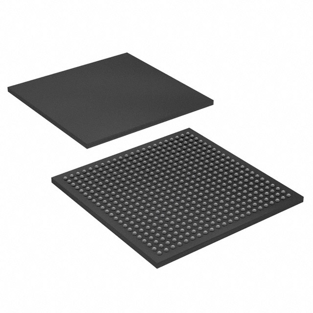
| Package / Case | 484-BBGA | Number of I/O | 291 | Voltage | 3 V - 3.6 V | ||
| Mounting Method | Surface Mount | RoHS Compliance | Unknown | REACH Compliance | REACH Unaffected | ||
| Moisture Sensitivity Level | 3 (168 Hours) | Number of LABs/CLBs | 360 | Number of Logic Elements/Cells | 2880 | ||
| Number of Gates | 116000 | ECCN | 3A001A2A | HTS Code | 8542.39.0001 | ||
| Qualification | N/A | Total RAM Bits | 20480 |
Overview of EPF10K50VFC484-1 – FLEX-10K® Field Programmable Gate Array (FPGA) IC 291 20480 2880 484-BBGA
The EPF10K50VFC484-1 is a member of the FLEX 10K embedded programmable logic family. It combines a dedicated logic array and embedded memory resources to enable System-on-a-Programmable-Chip (SOPC) integration and implementation of megafunctions such as efficient on-chip memory and specialized logic functions.
With 2,880 logic elements, approximately 20,480 bits of embedded RAM, and 291 I/O pins in a 484-ball BGA package, this commercial-grade device targets applications that require mid-density programmable logic, substantial embedded memory, and high I/O count within a 3.0–3.6 V supply environment.
Key Features
- Core logic — 2,880 logic elements and 360 logic array blocks (LABs) provide mid-range logic capacity for custom state machines, datapaths, and control logic.
- Embedded memory — Approximately 20,480 bits of on-chip RAM implemented across embedded array blocks (EABs) to support buffering, lookup tables, and memory-based megafunctions.
- I/O and interfacing — 291 user I/O pins enable high-pin-count designs for bridging, peripheral aggregation, and multiple parallel interfaces.
- System-level integration — Architecture supports SOPC-style integration and megafunctions for combining memory and logic on a single device.
- Reconfiguration and test — In-circuit reconfigurability via external configuration devices, intelligent controller, or JTAG; built-in JTAG boundary-scan test (BST) compliant with IEEE Std. 1149.1-1990 without consuming device logic.
- Clocking options — ClockLock and ClockBoost options and built-in low-skew clock distribution trees for optimized clocking and reduced skew.
- Power and supply — Operates from a 3.0 V to 3.6 V supply range; family-level documentation notes low-power standby characteristics for many FLEX 10K devices.
- Package and mounting — 484-ball FineLine BGA (23 × 23) package, surface mount, maximizing board space efficiency for compact system designs.
- Commercial temperature grade — Rated for 0 °C to 70 °C operating temperature and RoHS compliant.
Typical Applications
- Embedded control and SOPC integration — Use the device to implement customizable control logic and integrate memory-rich megafunctions for embedded systems.
- Memory-intensive logic — On-chip RAM supports buffering, FIFOs, and lookup tables for telecommunications, data-handling, or protocol processing functions.
- High-pin-count interface hubs — 291 I/O pins enable aggregation of multiple peripherals, sensor interfaces, or parallel bus bridging in compact board layouts.
- Field-updatable designs and prototyping — In-circuit reconfigurability and JTAG support facilitate iterative development, in-field updates, and manufacturing test integration.
Unique Advantages
- Highly integrated mid-density FPGA: Combines 2,880 logic elements with embedded RAM to reduce external component count and simplify system design.
- Substantial on-chip memory: Approximately 20,480 bits of embedded RAM across EABs supports memory-heavy functions without sacrificing logic capacity.
- Generous I/O capacity: 291 user I/O pins in a 484-ball BGA package enable flexible interfacing and high connector density on the board.
- In-system configurability and test: JTAG boundary-scan and multiple reconfiguration options streamline production test and allow in-field firmware updates.
- Clocking flexibility: Built-in low-skew distribution plus ClockLock/ClockBoost options help optimize timing for synchronous designs.
- Vendor toolchain support: The FLEX 10K family is supported by vendor development systems that provide automatic place-and-route and design entry for faster implementation.
Why Choose EPF10K50VFC484-1?
The EPF10K50VFC484-1 positions itself as a versatile mid-density FPGA for designs that need a balanced mix of logic, embedded memory, and high I/O in a compact BGA package. Its combination of 2,880 logic elements, approximately 20,480 bits of on-chip RAM, and 291 I/O makes it suited to embedded control, interface aggregation, and memory-backed logic functions within a 3.0–3.6 V supply environment.
Engineers and procurement teams looking for a reconfigurable, commercially graded solution with established family-level tool support and built-in JTAG test capability will find this device appropriate for scalable designs that benefit from on-board memory and flexible I/O while maintaining RoHS compliance.
Request a quote or submit an inquiry to purchase EPF10K50VFC484-1 and evaluate how its logic, memory, and I/O capabilities can fit your design requirements.


Date Founded: 1968
Headquarters: Santa Clara, California, USA
Employees: 130,000+
Revenue: $54.23 Billion
Certifications and Memberships: ISO9001:2015, ISO14001:2015, ISO17025:2017, ISO27001:2022, ISO45001:2018, ISO50001:2018


