
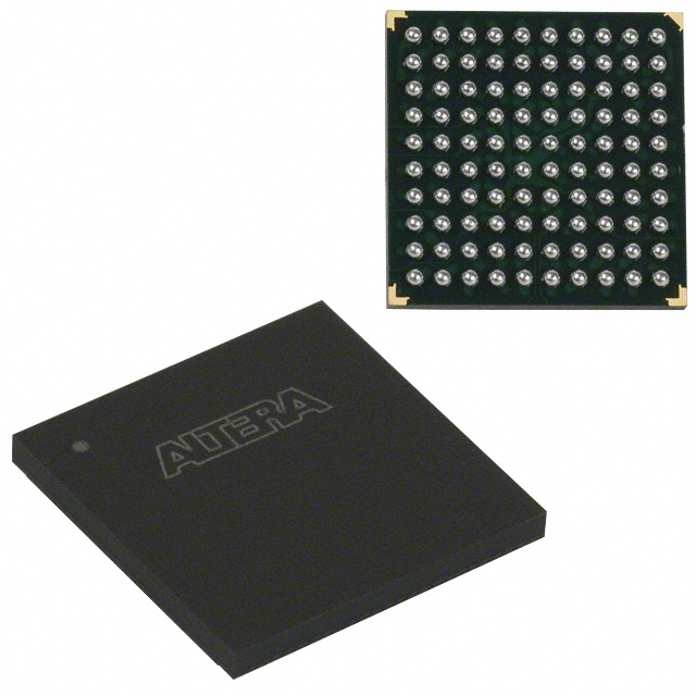
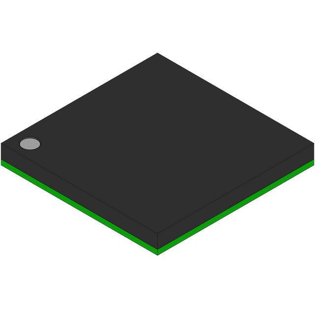
EPF6016AFC100-1
| Part Description |
FLEX 6000 Field Programmable Gate Array (FPGA) IC 81 1320 100-LBGA |
|---|---|
| Quantity | 429 Available (as of October 7, 2026) |
| Product Category | Field Programmable Gate Array (FPGA) |
|---|---|
| Manufacturer | Intel |
| Manufacturing Status | Obsolete |
| Manufacturer Standard Lead Time | Contact Us |
| Datasheet |
Specifications & Environmental
| Device Package | 100-FBGA (11x11) | Grade | Commercial | Operating Temperature | 0°C – 85°C | ||
|---|---|---|---|---|---|---|---|
| Package / Case | 100-LBGA | Number of I/O | 81 | Voltage | 3 V - 3.6 V | ||
| Mounting Method | Surface Mount | RoHS Compliance | Unknown | REACH Compliance | REACH Unaffected | ||
| Moisture Sensitivity Level | 3 (168 Hours) | Number of LABs/CLBs | 132 | Number of Logic Elements/Cells | 1320 | ||
| Number of Gates | 16000 | ECCN | 3A001A2A | HTS Code | 8542.39.0001 | ||
| Qualification | N/A |
Overview of EPF6016AFC100-1 – FLEX 6000 Field Programmable Gate Array (FPGA) IC 81 I/O 1320 Logic Elements 100-LBGA
The EPF6016AFC100-1 is a FLEX 6000 family FPGA packaged in a 100-ball BGA footprint and designed for commercial-grade programmable-logic applications. It uses a register-rich, look-up table (LUT) based architecture and the OptiFLEX architecture to increase device-area efficiency, making it suitable as a low-cost alternative to gate-array implementations and for rapid prototyping or design testing.
Key system-level capabilities described for the FLEX 6000 family include in-circuit reconfigurability, built-in JTAG boundary-scan, and flexible I/O options — features that support board-level integration, multi-voltage interfacing, and development workflows.
Key Features
- Logic Capacity — 1,320 logic elements and approximately 16,000 typical gates, providing a compact fabric for combinational and sequential logic.
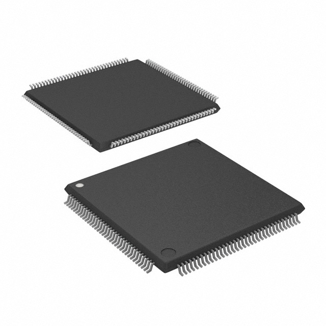
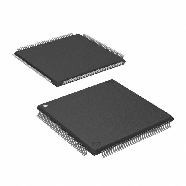
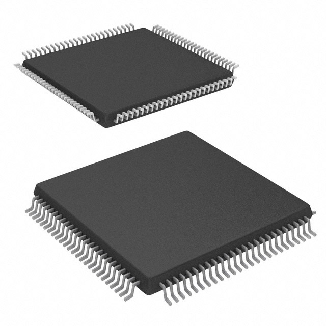
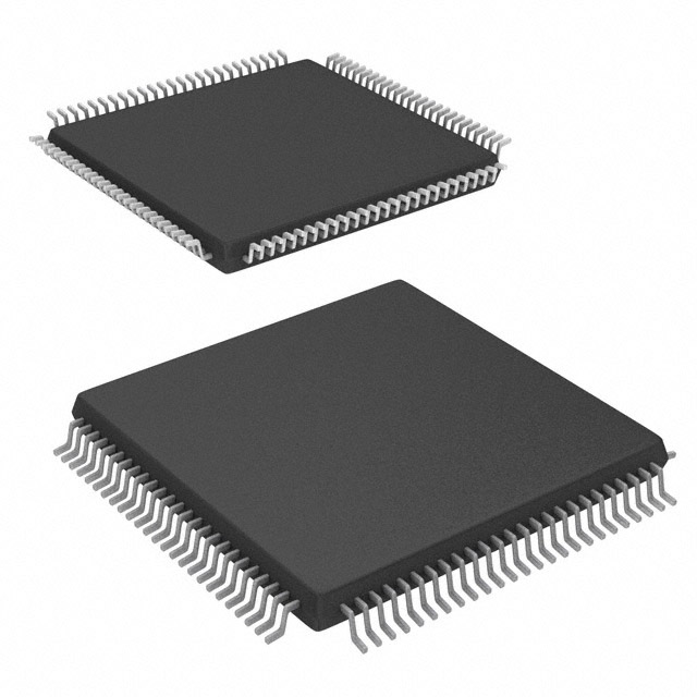
- I/O and Packaging — 81 I/O pins in a 100-ball fine-pitch BGA package (listed as 100-LBGA; supplier device package: 100-FBGA, 11×11), optimized for surface-mount assembly.
- Architecture — Register-rich, LUT-based core using the OptiFLEX architecture to improve area efficiency and routability.
- Clock and Routing — Built-in low-skew clock distribution tree and dedicated carry/cascade chains for implementing fast arithmetic and high-fan-in logic functions (automatic use by supported design tools).
- Configuration and Test — Supports in-circuit reconfigurability via external configuration device or intelligent controller; includes built-in IEEE Std. 1149.1-1990 JTAG boundary-scan circuitry and 100% functional testing at shipment.
- Power and Supply — Device supply range of 3 V to 3.6 V; commercial-grade operation with low standby power characteristics noted for the family.
- Thermal and Mounting — Surface-mount package rated for commercial temperature operation from 0 °C to 85 °C.
- Environment — RoHS compliant.
- Memory — Total on-chip RAM: 0 bits (device targets logic-centric implementations).
Typical Applications
- Prototyping and Design Testing — Rapidly iterate hardware designs and validate logic before committing to fixed gate-array production.
- Gate-Array Replacement — Implement low- to mid-density gate array functions with reprogrammable logic to reduce NRE and speed time-to-market.
- Interface Bridging and Glue Logic — Use flexible I/O and multi-voltage interfacing capabilities to bridge subsystems and implement board-level control logic.
- User Interface and Control — Deploy for custom control, sequencing, and peripheral management where compact logic density and reprogrammability are required.
Unique Advantages
- Compact, FPGA-based Gate-Array Alternative: Provides ~16,000 gates and 1,320 logic elements in a small 100-ball BGA footprint to replace custom gate arrays in lower-cost volumes.
- Efficient Core Architecture: OptiFLEX and a register-rich LUT structure improve area efficiency and routability for dense logic implementations.
- Board-Level Integration: 81 I/O pins and surface-mount BGA packaging simplify routing and EMI considerations on modern PCBs.
- Development and Test Support: Built-in JTAG boundary-scan and 100% functional testing assist production test and validation workflows.
- Flexible Configuration: In-circuit reconfigurability enables updating functionality in-system via external configuration devices or controllers.
- Toolflow Compatibility: Family documentation cites software design support and automatic place-and-route provided by vendor development tools, aiding implementation and verification.
Why Choose EPF6016AFC100-1?
The EPF6016AFC100-1 positions itself as a commercial-grade, logic-centric FPGA for designers seeking a reprogrammable alternative to gate-array designs and fast prototyping turnarounds. Its balance of 1,320 logic elements, 81 I/Os, OptiFLEX architecture, and BGA packaging make it suitable for compact boards that require flexible logic, interface bridging, and in-system reconfiguration.
Designed with production and development workflows in mind, the device benefits from family-level features such as JTAG boundary-scan, built-in low-skew clock distribution, and vendor-supplied design tools. These attributes make the part a pragmatic choice for teams focused on time-to-market, footprint efficiency, and iterative hardware development.
Request a quote or submit an inquiry to check availability and pricing for the EPF6016AFC100-1 and to discuss how it can fit your next programmable-logic design.





















Date Founded: 1968
Headquarters: Santa Clara, California, USA
Employees: 130,000+
Revenue: $54.23 Billion
Certifications and Memberships: ISO9001:2015, ISO14001:2015, ISO17025:2017, ISO27001:2022, ISO45001:2018, ISO50001:2018


