
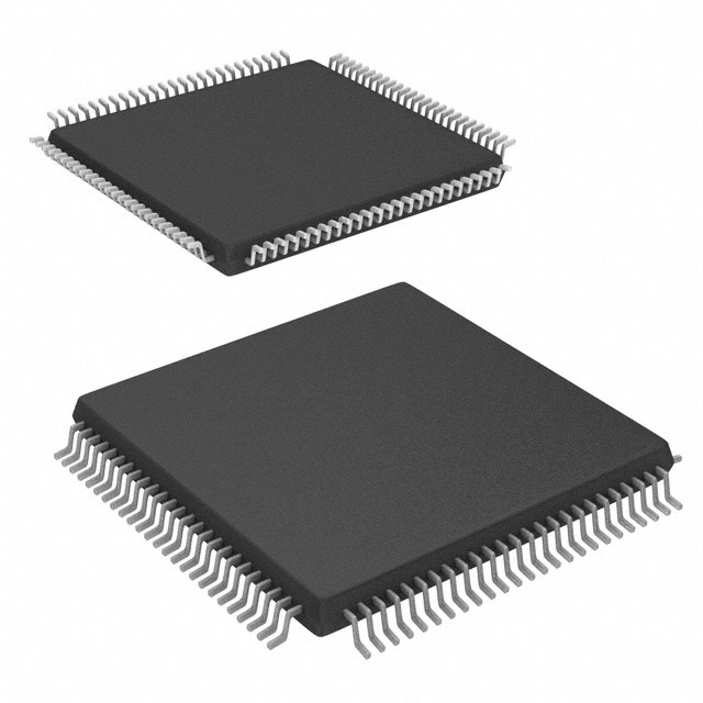
EPF6016ATC144-2
| Part Description |
FLEX 6000 Field Programmable Gate Array (FPGA) IC 117 1320 144-LQFP |
|---|---|
| Quantity | 1,059 Available (as of June 15, 2026) |

| Product Category | Field Programmable Gate Array (FPGA) |
|---|---|
| Manufacturer | Intel |
| Manufacturing Status | Obsolete |
| Manufacturer Standard Lead Time | Contact Us |
| Datasheet |
Specifications & Environmental
| Device Package | 144-TQFP (20x20) | Grade | Commercial | Operating Temperature | 0°C – 85°C | ||
|---|---|---|---|---|---|---|---|
| Package / Case | 144-LQFP | Number of I/O | 117 | Voltage | 3 V - 3.6 V | ||
| Mounting Method | Surface Mount | RoHS Compliance | RoHS non-compliant | REACH Compliance | REACH Unaffected | ||
| Moisture Sensitivity Level | 3 (168 Hours) | Number of LABs/CLBs | 132 | Number of Logic Elements/Cells | 1320 | ||
| Number of Gates | 16000 | ECCN | 3A991D | HTS Code | 8542.39.0001 | ||
| Qualification | N/A |
Overview of EPF6016ATC144-2 – FLEX 6000 Field Programmable Gate Array (FPGA) IC 117 1320 144-LQFP
The EPF6016ATC144-2 is a FLEX 6000 programmable logic device based on a register-rich, look-up table (LUT) architecture and Altera’s OptiFLEX structural optimizations. It provides reprogrammable SRAM-based logic suitable for mid-volume gate-array replacement, rapid prototyping, and system-level I/O glue and bridging.
With 1,320 logic elements and approximately 16,000 typical gates, 117 I/O pins and support for in-circuit reconfiguration, this 144-pin surface-mount device targets designs that need flexible logic, multi-voltage I/O interfacing, and compact package options at commercial temperature grades.
Key Features
- Core architecture Register-rich LUT-based architecture with OptiFLEX area-efficient implementation for compact programmable logic integration.
- Logic resources 1,320 logic elements and approximately 16,000 typical gates provide a solution for moderate-complexity programmable logic tasks.
- I/O capability 117 user I/O pins with individual tri-state output enable control and programmable output slew-rate control to optimize signal integrity and interfacing.
- In-circuit reconfigurability Supports in-circuit reconfiguration via an external configuration device or intelligent controller to enable field updates and iterative development.
- Dedicated arithmetic support Built-in carry and cascade chains accelerate adders, counters, and high-fan-in logic functions for common arithmetic and control tasks.
- Interconnect and clocking FastTrack interconnect structure for predictable routing delays and a built-in low-skew clock distribution tree for reliable timing across the device.
- Test and debug Built-in JTAG boundary-scan circuitry compliant with IEEE Std. 1149.1-1990, implemented without consuming user logic.
- Power and voltage Designed for 3.0 V to 3.6 V supply operation; low standby power (typical <0.5 mA) is documented for reduced idle consumption.
- Package and mounting 144-pin LQFP surface-mount package (supplier package: 144-TQFP 20×20) for compact PCB footprint and standard SMT assembly.
- Commercial grade and environmental Commercial operating range 0 °C to 85 °C and RoHS-compliant material status.
- Software and ecosystem Supported by FLEX 6000 device family design flows and automated place-and-route tools (as provided for the FLEX 6000 family).
Typical Applications
- Prototyping and design validation Reprogrammable SRAM logic and in-circuit reconfiguration make the device suited for iterative development and rapid hardware testing.
- Gate-array replacement for mid-volume products Provides a programmable alternative to fixed gate-array designs where post-manufacture changes or lower NRE are desired.
- Mixed-voltage system interfacing MultiVolt I/O interface capability enables bridging between subsystems operating at different voltage levels.
- System glue and I/O control Use the available I/O and dedicated arithmetic resources for protocol glue logic, peripheral interfacing, and simple control functions.
Unique Advantages
- Flexible, reprogrammable logic: SRAM-based LUT architecture lets you change functionality during prototyping or in the field via in-circuit reconfiguration.
- Compact integration: OptiFLEX architecture and 1,320 logic elements deliver a balance of density and routability for space-constrained designs.
- Rich I/O and control: 117 I/O pins with individual enable and programmable slew-rate control help optimize board-level signal performance and reduce external components.
- Built-in testability: IEEE 1149.1-compliant boundary-scan reduces the need for additional test logic while simplifying board-level test strategies.
- Scalable family support: SameFrame pin-compatibility across FLEX 6000 devices in the same package family enables migration between densities without changing PCB footprints.
- Low idle power: Documented low standby current (typical <0.5 mA) supports designs that require reduced power in idle or standby modes.
Why Choose EPF6016ATC144-2?
The EPF6016ATC144-2 positions itself as a versatile, reprogrammable logic device for designers who need a low-cost alternative to fixed gate-array solutions, combined with the flexibility of in-circuit reconfiguration. Its combination of 1,320 logic elements, approximately 16,000 gates, and 117 I/O pins in a 144-LQFP package delivers a practical balance of integration, I/O capability, and board-level density for commercial-temperature applications.
Supported by the FLEX 6000 family design flows and featuring built-in JTAG boundary-scan and dedicated arithmetic/cascade resources, this device suits teams focused on rapid iteration, mixed-voltage interfacing, and compact system-level logic integration while retaining the option to scale across the FLEX 6000 device family.
Request a quote or submit your requirements to get pricing and availability for the EPF6016ATC144-2.


Date Founded: 1968
Headquarters: Santa Clara, California, USA
Employees: 130,000+
Revenue: $54.23 Billion
Certifications and Memberships: ISO9001:2015, ISO14001:2015, ISO17025:2017, ISO27001:2022, ISO45001:2018, ISO50001:2018


