
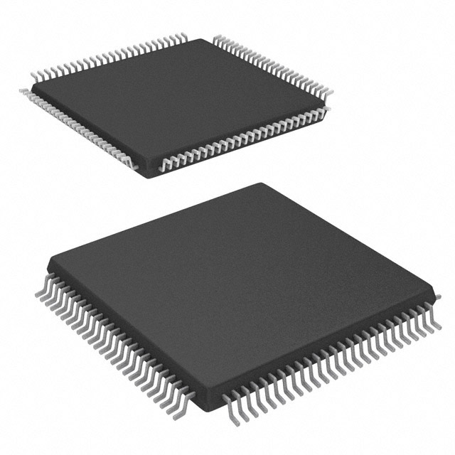
EPF6016ATC144-3N
| Part Description |
FLEX 6000 Field Programmable Gate Array (FPGA) IC 117 1320 144-LQFP |
|---|---|
| Quantity | 521 Available (as of June 14, 2026) |

| Product Category | Field Programmable Gate Array (FPGA) |
|---|---|
| Manufacturer | Intel |
| Manufacturing Status | Obsolete |
| Manufacturer Standard Lead Time | Contact Us |
| Datasheet |
Specifications & Environmental
| Device Package | 144-TQFP (20x20) | Grade | Commercial | Operating Temperature | 0°C – 85°C | ||
|---|---|---|---|---|---|---|---|
| Package / Case | 144-LQFP | Number of I/O | 117 | Voltage | 3 V - 3.6 V | ||
| Mounting Method | Surface Mount | RoHS Compliance | Unknown | REACH Compliance | REACH Unaffected | ||
| Moisture Sensitivity Level | 3 (168 Hours) | Number of LABs/CLBs | 132 | Number of Logic Elements/Cells | 1320 | ||
| Number of Gates | 16000 | ECCN | 3A991D | HTS Code | 8542.39.0001 | ||
| Qualification | N/A |
Overview of EPF6016ATC144-3N – FLEX 6000 FPGA IC, 117 I/O, 1,320 Logic Elements, 144-LQFP
The EPF6016ATC144-3N is a FLEX 6000 family field-programmable gate array (FPGA) provided by Intel. Based on a register-rich, lookup-table (LUT) architecture and the OptiFLEX layout, this device offers a reconfigurable SRAM-based implementation suitable for prototype and low-cost production designs.
With 1,320 logic elements (approximately 16,000 typical gates) and 117 user I/O pins in a 144-pin LQFP package, the EPF6016ATC144-3N targets commercial applications requiring flexible logic integration, in-circuit reconfigurability and predictable I/O control over a standard commercial operating range.
Key Features
- Core Logic 1,320 logic elements and a typical gate count of 16,000 provide programmable combinational and sequential logic capacity for glue logic, state machines and custom processing functions.
- OptiFLEX Architecture OptiFLEX layout and a register-rich LUT-based architecture increase area efficiency and support fast design iteration through reconfigurable SRAM elements.
- I/O and Signal Control 117 user I/O pins with individual tri-state output enable control and programmable output slew-rate to manage switching noise and interface timing.
- Routing and Arithmetic Support FastTrack interconnect, dedicated carry and cascade chains enable efficient implementation of arithmetic functions, adders, counters and high-fan-in logic structures.
- System-Level Capabilities In-circuit reconfigurability (ICR) via an external configuration device or intelligent controller and built-in IEEE 1149.1 JTAG boundary-scan for board-level testability.
- Clocking and Global Signals Built-in low-skew clock distribution tree and four low-skew global paths for clock, clear, preset or logic signals to support synchronous designs.
- Electrical & Packaging Commercial-grade, surface-mount 144-LQFP package (supplier package: 144-TQFP, 20×20 mm) with supply voltage range 3.0 V to 3.6 V and operating temperature 0 °C to 85 °C.
- Quality and Compliance 100% functional testing before shipment and RoHS compliance for environmental compatibility.
Typical Applications
- Prototyping and Design Validation Reconfigurable SRAM elements and in-circuit reconfiguration make the device suitable for rapid prototyping and iterative design testing.
- Interface and Glue Logic Use the programmable I/O and per-pin control to implement protocol bridging, bus interfacing and custom peripheral handlers.
- Embedded Control and State Machines The register-rich LUT architecture and dedicated arithmetic chains are well suited for control logic, finite-state machines and real-time decision logic.
- Board-Level Test and Debug Built-in JTAG boundary-scan simplifies board-level testing and manufacturing diagnostics without consuming user logic.
Unique Advantages
- Balanced Logic Density: 1,320 logic elements (≈16,000 typical gates) provide a predictable capacity for mid-density programmable designs.
- Flexible I/O Management: 117 I/O pins with individual tri-state and slew-rate control reduce external buffering and simplify interface timing control.
- In-Circuit Reconfigurability: Support for ICR via external configuration devices enables field updates and functional changes after deployment.
- Deterministic Routing: FastTrack interconnect and dedicated carry/cascade chains yield efficient placement of arithmetic and high-fan-in logic, improving performance predictability.
- Commercial Temperature and Supply Range: Designed for 3.0 V to 3.6 V operation and 0 °C to 85 °C ambient, matching standard commercial embedded applications.
- Testability and Compliance: IEEE 1149.1 JTAG boundary-scan and 100% functional testing support manufacturing yield and board-level diagnostics.
Why Choose EPF6016ATC144-3N?
The EPF6016ATC144-3N positions itself as a flexible, commercially graded FPGA option for designers who need mid-range programmable logic density, robust I/O control and the ability to reconfigure designs in-circuit. Its OptiFLEX/LUT architecture and dedicated routing features make it suitable for prototyping, interface logic and embedded control tasks where predictable routing and arithmetic support matter.
With a standard 144-LQFP footprint, RoHS compliance, and full device testing, this part delivers a practical combination of integration, testability and field flexibility for commercial embedded systems and production designs that rely on in-place reprogrammability and board-level diagnostics.
Request a quote or submit a purchase request today to evaluate the EPF6016ATC144-3N for your next programmable logic design.


Date Founded: 1968
Headquarters: Santa Clara, California, USA
Employees: 130,000+
Revenue: $54.23 Billion
Certifications and Memberships: ISO9001:2015, ISO14001:2015, ISO17025:2017, ISO27001:2022, ISO45001:2018, ISO50001:2018


