
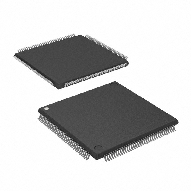
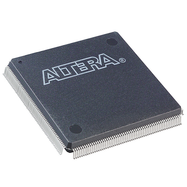
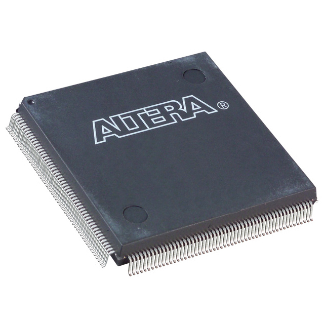
EPF6024AQC240-3
| Part Description |
FLEX 6000 Field Programmable Gate Array (FPGA) IC 199 1960 240-BFQFP |
|---|---|
| Quantity | 584 Available (as of June 15, 2026) |

| Product Category | Field Programmable Gate Array (FPGA) |
|---|---|
| Manufacturer | Intel |
| Manufacturing Status | Obsolete |
| Manufacturer Standard Lead Time | Contact Us |
| Datasheet |
Specifications & Environmental
| Device Package | 240-PQFP (32x32) | Grade | Commercial | Operating Temperature | 0°C – 85°C | ||
|---|---|---|---|---|---|---|---|
| Package / Case | 240-BFQFP | Number of I/O | 199 | Voltage | 3 V - 3.6 V | ||
| Mounting Method | Surface Mount | RoHS Compliance | RoHS non-compliant | REACH Compliance | REACH Unaffected | ||
| Moisture Sensitivity Level | 3 (168 Hours) | Number of LABs/CLBs | 196 | Number of Logic Elements/Cells | 1960 | ||
| Number of Gates | 24000 | ECCN | 3A991D | HTS Code | 8542.39.0001 | ||
| Qualification | N/A |
Overview of EPF6024AQC240-3 – FLEX 6000 Field Programmable Gate Array (FPGA) IC 199 I/Os 240-BFQFP
The EPF6024AQC240-3 is a FLEX 6000 family FPGA featuring the OptiFLEX LUT-based architecture and register-rich logic. It provides a reprogrammable, low-cost alternative to high-volume gate array designs and is targeted at prototyping, design testing, and low- to mid-volume programmable logic applications.
With 1,960 logic elements (approximately 24,000 typical gates), 199 I/O pins, and support for in-circuit reconfiguration and IEEE-1149.1 JTAG boundary-scan, this device balances moderate logic density, flexible I/O, and system-level configurability for embedded and control-oriented designs.
Key Features
- Core Architecture — OptiFLEX register-rich, LUT-based architecture designed to improve device area efficiency and routing.
- Logic Capacity — 1,960 logic elements delivering approximately 24,000 typical gates for implementing combinational and sequential logic.
- I/O and Interface Capabilities — 199 I/O pins with per-pin tri-state output enable and programmable output slew-rate control for optimized signal integrity and interface flexibility.
- Configuration & Test — In-circuit reconfigurability via external configuration device or intelligent controller; built-in IEEE Std. 1149.1 JTAG boundary-scan (BST) circuitry for board-level test and programming without consuming user logic.
- Interconnect & Arithmetic Support — FastTrack continuous routing structure, dedicated carry and cascade chains to implement arithmetic and high-fan-in logic functions efficiently.
- Power and Voltage — Supply voltage 3.0 V to 3.6 V; low-power standby behavior is supported by the FLEX 6000 family architecture.
- Package & Mounting — Surface-mount device in a 240-pin BFQFP package (product lists Package Case: 240-BFQFP and Supplier Device Package: 240-PQFP (32×32)).
- Commercial Temperature Rating — Rated for 0 °C to 85 °C operation suitable for commercial applications.
- No Embedded SRAM — Total on-chip RAM bits: 0, for designs that rely on external memory or do not require embedded RAM.
- Design Tool Support — FLEX 6000 family devices are supported by software design flows that provide automatic place-and-route and industry-standard design-entry formats.
Typical Applications
- Prototype and Design Validation — Rapidly iterate hardware logic and verify system behavior during development thanks to the device’s reprogrammability and JTAG support.
- Low- to Mid-Volume Gate Array Replacement — Implement custom logic without the cost and lead time of ASIC gate arrays while retaining the ability to change designs in the field.
- Interface Bridging & Glue Logic — Use the device’s flexible I/O and programmable routing to bridge peripherals or implement board-level glue logic between subsystems operating at different voltages.
- Control and Sequencing — Implement control state machines, counters, and arithmetic functions using dedicated carry and cascade chains for efficient resource use.
Unique Advantages
- Reprogrammable Flexibility: In-circuit reconfiguration enables design updates and functional changes without hardware replacement.
- Balanced Logic Density: 1,960 logic elements (~24,000 gates) provide substantial capability for complex glue logic and mid-size designs while maintaining manageable power and footprint.
- Comprehensive I/O: 199 I/O pins with per-pin control and slew-rate programmability simplify signal interfacing and help control switching noise.
- Built-in Testability: IEEE-1149.1 JTAG boundary-scan facilitates board-level testing and in-field diagnostics without consuming user logic resources.
- Efficient Arithmetic Support: Dedicated carry and cascade chains accelerate adders, counters, and high-fan-in functions to improve performance for common logic patterns.
- Commercial Readiness: Surface-mount 240-pin package and 0 °C to 85 °C rating suit a wide range of commercial embedded systems and production environments.
Why Choose EPF6024AQC240-3?
The EPF6024AQC240-3 is positioned for engineers and teams seeking a reprogrammable, mid-density FPGA solution with strong I/O capability and family-level architecture advantages such as OptiFLEX and dedicated arithmetic chains. Its combination of 1,960 logic elements, nearly 24,000 typical gates, and 199 I/Os makes it well suited to prototyping, design validation, and replacing low- to mid-volume gate array implementations.
With commercial temperature grading, support for in-circuit reconfiguration and JTAG boundary-scan, and a compact 240-pin surface-mount package, this device provides a practical balance of integration, configurability, and system-level testability for embedded product development and small-batch production.
Request a quote or submit your requirements to get pricing and availability for the EPF6024AQC240-3 and evaluate how it fits into your next programmable-logic design.


Date Founded: 1968
Headquarters: Santa Clara, California, USA
Employees: 130,000+
Revenue: $54.23 Billion
Certifications and Memberships: ISO9001:2015, ISO14001:2015, ISO17025:2017, ISO27001:2022, ISO45001:2018, ISO50001:2018


