
M1AFS250-FG256
| Part Description |
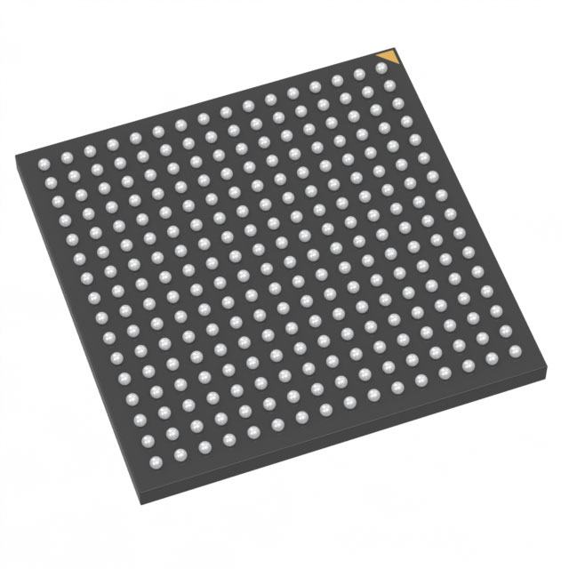
Fusion® Field Programmable Gate Array (FPGA) IC 114 36864 256-LBGA |
|---|---|
| Quantity | 62 Available (as of June 10, 2026) |

| Product Category | Field Programmable Gate Array (FPGA) |
|---|---|
| Manufacturer | Microchip Technology |
| Manufacturing Status | Active |
| Manufacturer Standard Lead Time | 16 Weeks |
| Datasheet |
Specifications & Environmental
| Device Package | 256-FPBGA (17x17) | Grade | Commercial | Operating Temperature | 0°C – 85°C | ||
|---|---|---|---|---|---|---|---|
| Package / Case | 256-LBGA | Number of I/O | 114 | Voltage | 1.425 V - 1.575 V | ||
| Mounting Method | Surface Mount | RoHS Compliance | RoHS non-compliant | REACH Compliance | REACH Unaffected | ||
| Moisture Sensitivity Level | 3 (168 Hours) | Number of LABs/CLBs | 6144 | Number of Logic Elements/Cells | 6144 | ||
| Number of Gates | 250000 | ECCN | 3A991D | HTS Code | 8542.39.0001 | ||
| Qualification | N/A | Total RAM Bits | 36864 |
Overview of M1AFS250-FG256 – Fusion Field Programmable Gate Array (FPGA) IC, 114 I/O, 256-LBGA
The M1AFS250-FG256 is a Fusion® Field Programmable Gate Array (FPGA) IC from Microchip Technology. It integrates 6,144 logic elements, approximately 36,864 bits of embedded RAM, and a 114-pin I/O count in a compact 256-LBGA package.
Designed for commercial-grade embedded designs, the device operates from a 1.425 V to 1.575 V supply and across an operating temperature range of 0 °C to 85 °C. Its surface-mount 256-FPBGA (17×17) packaging and RoHS compliance support space-efficient board integration and environmental compliance requirements.
Key Features
- Core Logic Provides 6,144 logic elements (CLBs) to implement custom digital functions and combinational/sequential logic structures.
- Embedded Memory Includes 36,864 bits of on-chip RAM (approximately 0.037 Mbits) for data buffering, state storage, and small memory structures.
- I/O Capacity 114 general-purpose I/O pins suitable for interfacing with peripherals, sensors, and other digital logic blocks.
- Gate Count Approximately 250,000 gates enabling integration of moderate-complexity logic and glue functions on a single device.
- Power Operates from a supply voltage range of 1.425 V to 1.575 V, supporting designs targeting that core voltage domain.
- Package & Mounting Delivered in a 256-LBGA package (supplier device package: 256-FPBGA, 17×17) with surface-mount mounting for compact PCB layouts.
- Temperature & Grade Commercial grade operation from 0 °C to 85 °C, suitable for standard commercial applications.
- Environmental Compliance RoHS compliant to meet common environmental and materials requirements.
Typical Applications
- Embedded Control Implement control logic and state machines using the device’s 6,144 logic elements and on-chip RAM for small data storage.
- Interface Bridging Use the 114 I/O pins to bridge and translate between digital peripherals and system buses in compact designs.
- Custom Digital Functions Integrate glue logic, protocol handling, or application-specific accelerators leveraging the 250,000-gate equivalence.
- Prototyping & Development Evaluate custom logic implementations in a surface-mount 256-LBGA package suited for lab and prototype boards.
Unique Advantages
- Balanced logic and memory footprint: 6,144 logic elements combined with 36,864 bits of embedded RAM provide a midpoint capacity for moderate-complexity designs.
- Generous I/O availability: 114 I/O pins let you connect multiple peripherals, sensors, and interfaces without immediate need for external I/O expanders.
- Compact package: 256-LBGA (256-FPBGA, 17×17) supports high-density board layouts while keeping the FPGA footprint small.
- Commercial temperature rating: 0 °C to 85 °C operation aligns with standard commercial electronics use cases.
- Controlled supply domain: Defined 1.425 V–1.575 V supply range simplifies power-rail planning for designs targeting that core voltage.
- Regulatory readiness: RoHS compliance supports environmentally conscious product requirements.
Why Choose M1AFS250-FG256?
The M1AFS250-FG256 positions itself as a compact, commercially rated FPGA option that combines a mid-range logic element count with on-chip memory and a substantial I/O complement. It is well suited for designers who need to consolidate moderate-complexity digital functions into a single, surface-mount 256-LBGA device while adhering to standard commercial temperature and RoHS requirements.
This part is ideal for teams developing embedded control, interface bridging, and custom digital logic where board space, I/O density, and a defined supply voltage range are key design considerations. Its specification set supports straightforward integration into commercial electronic products with predictable thermal and electrical envelopes.
Request a quote or submit an inquiry to obtain pricing and availability for the M1AFS250-FG256 and to discuss how it fits your next design.


Date Founded: 1989
Headquarters: Chandler, Arizona, USA
Employees: 22,000+
Revenue: $8.349 Billion
Certifications and Memberships: ISO9001:2015, IATF16949:2016, AS 9100D


