
XA6SLX75-2FGG484Q
| Part Description |
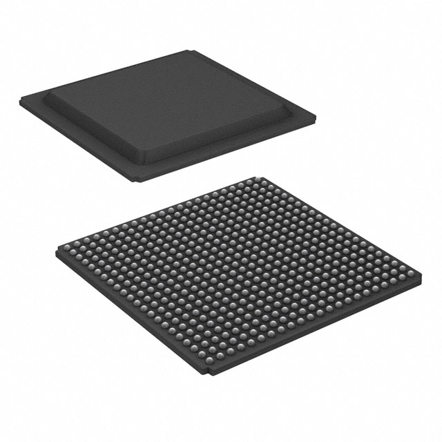
Spartan®-6 LX XA Field Programmable Gate Array (FPGA) IC 280 3170304 74637 484-BBGA |
|---|---|
| Quantity | 1,774 Available (as of October 8, 2026) |
| Product Category | Field Programmable Gate Array (FPGA) |
|---|---|
| Manufacturer | AMD |
| Manufacturing Status | Active |
| Manufacturer Standard Lead Time | 12 Weeks |
| Datasheet |
Specifications & Environmental
| Device Package | 484-FBGA (23x23) | Grade | Automotive | Operating Temperature | -40°C – 125°C | ||
|---|---|---|---|---|---|---|---|
| Package / Case | 484-BBGA | Number of I/O | 280 | Voltage | 1.14 V - 1.26 V | ||
| Mounting Method | Surface Mount | RoHS Compliance | ROHS3 Compliant | REACH Compliance | REACH Unaffected | ||
| Moisture Sensitivity Level | 3 (168 Hours) | Number of LABs/CLBs | 5831 | Number of Logic Elements/Cells | 74637 | ||
| Number of Gates | N/A | ECCN | 3A991D | HTS Code | 8542.39.0001 | ||
| Qualification | AEC-Q100 | Total RAM Bits | 3170304 |
Overview of XA6SLX75-2FGG484Q – Spartan®-6 LX XA Field Programmable Gate Array (FPGA), 484-BBGA
The XA6SLX75-2FGG484Q is a Spartan®-6 LX XA Field Programmable Gate Array (FPGA) IC offering high logic density and on-chip memory in a compact ball-grid array package. It is a programmable logic device designed for applications that require substantial logic resources, embedded memory, and a large number of configurable I/O connections.
With a broad operating temperature range and AEC-Q100 qualification, this device targets applications where reliability and qualification matter, while providing a balance of logic capacity, I/O count, and power characteristics suitable for system-level integration.
Key Features
- Logic Capacity Approximately 74,637 logic elements provide significant resources for custom digital logic, finite state machines, and parallel processing implementations.
- Configurable Logic Blocks (CLBs) 5,831 CLBs enable structured placement of logic for deterministic design scaling.
- Embedded Memory Approximately 3.17 Mbits of on-chip RAM support local data buffering, FIFOs, and state storage without external memory.
- I/O Density 280 programmable I/O pins allow extensive interfacing to sensors, peripherals, and external buses.
- Power Core supply range of 1.14 V to 1.26 V supports low-voltage system architectures.
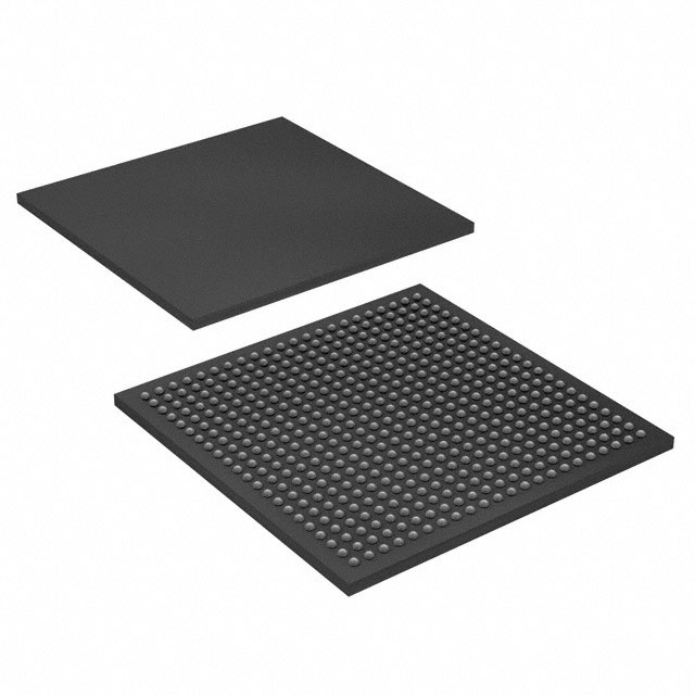
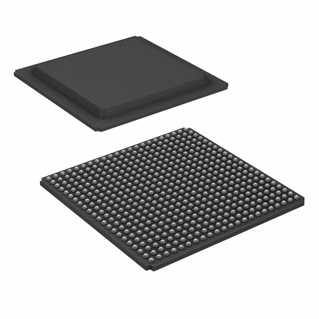
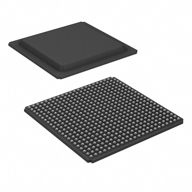
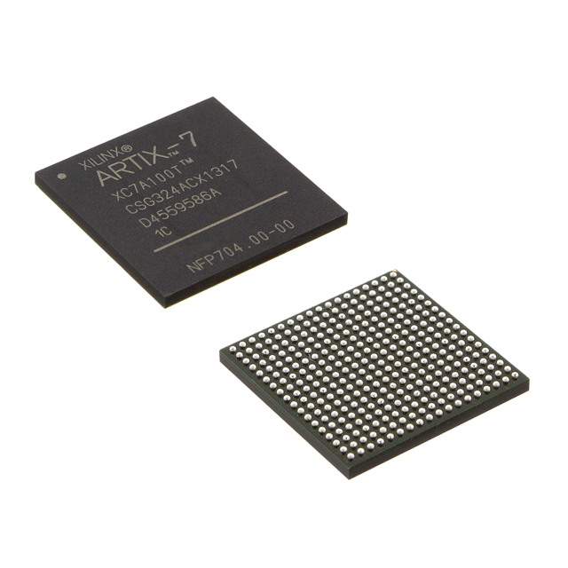
- Package & Mounting 484-BBGA package (supplier device package: 484-FBGA, 23×23) in a surface-mount format for compact board layouts.
- Qualification & Temperature Range Automotive grade with AEC-Q100 qualification and an operating temperature range of –40 °C to 125 °C for environments requiring qualified components.
- Environmental Compliance RoHS compliant to meet lead-free and hazardous-substance requirements.
Typical Applications
- Automotive control systems AEC-Q100 qualification and a –40 °C to 125 °C operating range make this FPGA suitable for in-vehicle control logic, sensor interfacing, and data aggregation tasks that require qualified silicon.
- Custom signal processing Approximately 74,637 logic elements and 3.17 Mbits of embedded memory enable implementation of bespoke signal-processing pipelines, buffering, and protocol handling on-chip.
- Interface consolidation and bridging With 280 I/O pins, the device can consolidate multiple peripheral interfaces and implement protocol bridging without extensive external logic.
- Embedded system integration Compact 484-BBGA surface-mount packaging and low core voltage simplify integration into space-constrained boards and modern low-voltage designs.
Unique Advantages
- High logic and memory integration: Combines substantial logic resources with approximately 3.17 Mbits of embedded RAM to reduce dependence on external memory and discrete logic devices.
- Qualified for automotive environments: AEC‑Q100 qualification and extended temperature range support designs that require industry-recognized qualification and thermal robustness.
- Large, flexible I/O complement: 280 I/O pins provide designers with broad connectivity options to simplify board-level interfacing and reduce the need for additional IO expanders.
- Compact, surface-mount BBGA package: The 484-ball FBGA (23×23) footprint enables high-density board placement while maintaining a reliable solderable package.
- Low-voltage core operation: 1.14 V to 1.26 V core supply aligns with modern low-voltage system domains and power budgets.
- RoHS compliant: Meets environmental and manufacturing requirements for lead‑free assemblies.
Why Choose XA6SLX75-2FGG484Q?
The XA6SLX75-2FGG484Q positions itself as a high-capacity, qualified FPGA option for designs that require a balance of logic density, embedded memory, and extensive I/O in a compact package. Its AEC‑Q100 qualification and wide operating temperature range make it suitable for applications where component qualification and thermal tolerance are required.
This device is well suited to engineers building complex embedded systems, automotive control modules, and interface- or processing-heavy applications that need on-chip resources to minimize external components and simplify system architecture. The combination of logic capacity, memory, and I/O delivers a scalable, reliable building block that supports long-term design lifecycles.
Request a quote or submit an inquiry for XA6SLX75-2FGG484Q to check availability, lead times, and pricing for your next design.























Date Founded: 1969
Headquarters: Santa Clara, California, USA
Employees: 25,000+
Revenue: $22.68 Billion
Certifications and Memberships: ISO9001:2015, RoHS, REACH











