
XC2V1500-4FF896I
| Part Description |
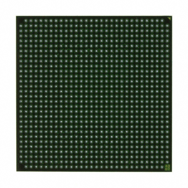
Virtex®-II Field Programmable Gate Array (FPGA) IC 528 884736 896-BBGA, FCBGA |
|---|---|
| Quantity | 472 Available (as of June 18, 2026) |

| Product Category | Field Programmable Gate Array (FPGA) |
|---|---|
| Manufacturer | AMD |
| Manufacturing Status | Obsolete |
| Manufacturer Standard Lead Time | Contact Us |
| Datasheet |
Specifications & Environmental
| Device Package | 896-FCBGA (31x31) | Grade | Industrial | Operating Temperature | -40°C – 100°C | ||
|---|---|---|---|---|---|---|---|
| Package / Case | 896-BBGA, FCBGA | Number of I/O | 528 | Voltage | 1.425 V - 1.575 V | ||
| Mounting Method | Surface Mount | RoHS Compliance | RoHS non-compliant | REACH Compliance | REACH Unaffected | ||
| Moisture Sensitivity Level | 4 (72 Hours) | Number of LABs/CLBs | 1920 | Number of Logic Elements/Cells | 17280 | ||
| Number of Gates | 1500000 | ECCN | 3A001A7A | HTS Code | 8542.39.0001 | ||
| Qualification | N/A | Total RAM Bits | 884736 |
Overview of XC2V1500-4FF896I – Virtex-II FPGA, 1.5M gates, 896-FCBGA
The XC2V1500-4FF896I is a Virtex®-II platform field programmable gate array supplied in a 896-FCBGA (31×31) package. It delivers 1,500,000 system gates realized as approximately 17,280 logic elements, with approximately 0.88 Mbits of embedded RAM and 528 user I/O pins.
Designed for industrial-grade applications, this surface-mount FPGA supports a 1.425 V to 1.575 V core supply and an operating temperature range of -40°C to 100°C. The device incorporates Virtex-II platform capabilities such as the SelectRAM™ memory hierarchy, dedicated 18×18 multiplier resources, Digital Clock Manager (DCM) functionality and high-performance SelectIO™ interfaces for demanding logic, memory and I/O tasks.
Key Features
- Logic Capacity Approximately 17,280 logic elements supporting a total of 1,500,000 system gates for complex combinational and sequential designs.
- Embedded Memory Approximately 0.88 Mbits of on-chip RAM (total RAM bits: 884,736) for large buffering, state storage and distributed memory structures.
- I/O Density & Standards 528 user I/Os delivered through the 896-FCBGA package to support wide data buses and multi‑channel interfaces.
- Dedicated Arithmetic Resources Platform includes 18-bit × 18-bit multiplier resources suitable for arithmetic and DSP-oriented functions.
- Clock Management Incorporates Digital Clock Manager (DCM) capabilities from the Virtex-II platform for phase shifting and deskewing in clock-critical designs.
- Package & Mounting 896-FCBGA (31×31) flip‑chip BGA package, surface-mount mounting for compact board integration.
- Power Core supply voltage range: 1.425 V to 1.575 V, enabling consistent power planning for the FPGA core.
- Temperature & Grade Industrial-grade device rated for operation from -40°C to 100°C.
- Environmental Compliance RoHS compliant.
Typical Applications
- High‑performance memory interfaces Use the device’s selectable memory hierarchy and abundant I/O to implement SDR/DDR and other external memory controllers and bridge functions.
- DSP and arithmetic‑intensive processing Leverage the integrated 18×18 multipliers and significant logic capacity for signal processing, filtering and computational accelerators.
- High‑density programmable logic Deploy as a central programmable fabric for protocol handling, custom logic blocks and system control where large logic and memory resources are required.
- Wide parallel I/O systems 528 I/Os enable multi-channel data acquisition, aggregation and routing applications that demand extensive external connectivity.
Unique Advantages
- Balanced logic and memory integration: The combination of ~17,280 logic elements and ~0.88 Mbits of embedded RAM supports mixed compute-and-buffer architectures without excessive external memory dependence.
- High I/O count for system integration: 528 user I/Os in a single FCBGA package reduce the need for external interface components and simplify board-level routing for wide-bus designs.
- Industrial temperature rating: Operation from -40°C to 100°C suits deployments that require robust thermal performance.
- Compact, manufacturable package: 896‑FCBGA (31×31) form factor supports high-density assembly and surface-mount production processes.
- Deterministic clocking and arithmetic support: Platform-level DCMs and dedicated multipliers enable precise clock control and efficient implementation of arithmetic-heavy logic.
- Regulatory and environmental readiness: RoHS compliance simplifies integration into modern product flows with environmental standards in mind.
Why Choose XC2V1500-4FF896I?
The XC2V1500-4FF896I positions itself as a versatile Virtex-II FPGA option where substantial logic, embedded memory and a high pin count are required in an industrial-grade package. Its combination of approximately 1.5M system gates, ~17,280 logic elements, and ~0.88 Mbits of RAM supports complex control, interfacing and processing tasks within a compact 896-FCBGA footprint.
This device is well suited for engineers and product teams building systems that need integrated arithmetic resources, reliable clock management, and broad external connectivity while maintaining RoHS compliance and industrial temperature tolerance. Its platform heritage and on-chip resources deliver long-term design scalability and predictable integration into established FPGA-based workflows.
Request a quote or submit an RFQ to check current pricing and availability for the XC2V1500-4FF896I.


Date Founded: 1969
Headquarters: Santa Clara, California, USA
Employees: 25,000+
Revenue: $22.68 Billion
Certifications and Memberships: ISO9001:2015, RoHS, REACH


