
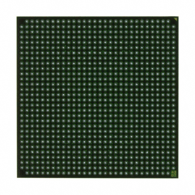
XC2V1500-4FGG676C
| Part Description |
Virtex®-II Field Programmable Gate Array (FPGA) IC 392 884736 676-BGA |
|---|---|
| Quantity | 318 Available (as of October 7, 2026) |

| Product Category | Field Programmable Gate Array (FPGA) |
|---|---|
| Manufacturer | AMD |
| Manufacturing Status | Obsolete |
| Manufacturer Standard Lead Time | Contact Us |
| Datasheet |
Specifications & Environmental
| Device Package | 676-FBGA (27x27) | Grade | Commercial | Operating Temperature | 0°C – 85°C | ||
|---|---|---|---|---|---|---|---|
| Package / Case | 676-BGA | Number of I/O | 392 | Voltage | 1.425 V - 1.575 V | ||
| Mounting Method | Surface Mount | RoHS Compliance | Unknown | REACH Compliance | REACH Unaffected | ||
| Moisture Sensitivity Level | 3 (168 Hours) | Number of LABs/CLBs | 1920 | Number of Logic Elements/Cells | 17280 | ||
| Number of Gates | 1500000 | ECCN | 3A991D | HTS Code | 8542.39.0001 | ||
| Qualification | N/A | Total RAM Bits | 884736 |
Overview of XC2V1500-4FGG676C – Virtex®-II Field Programmable Gate Array (FPGA) IC 392 884736 676-BGA
The XC2V1500-4FGG676C is a Virtex®-II platform FPGA offered in a 676-ball fine-pitch BGA (27×27) package. It delivers a high-density programmable fabric with configurable logic, embedded memory, dedicated multiplier blocks and extensive I/O suitable for complex digital designs.
This device targets applications requiring large logic capacity, significant on-chip RAM and flexible high-speed interfacing. Its core value proposition is integration of logic, memory and I/O in a compact surface-mount package with industry-standard supply and operating ranges.
Key Features
- Configurable Logic 1,920 configurable logic blocks (CLBs) providing approximately 17,280 logic elements for implementing complex custom logic functions.
- Embedded Memory Total on-chip RAM of 884,736 bits — approximately 0.885 Mbits of embedded memory for packet buffering, FIFOs and state storage.
- SelectRAM Memory Hierarchy (series-level) Virtex-II platform memory architecture includes SelectRAM resources with up to 18-Kbit blocks and series-level capability of up to 3 Mb of dual-port RAM in block resources.
- Dedicated Arithmetic Blocks (series-level) 18-bit × 18-bit multiplier blocks are available on the Virtex-II platform for efficient arithmetic and DSP implementations.
- I/O Capacity 392 user I/Os available in the 676-FBGA package to support wide parallel interfaces and mixed signaling needs.
- System Gates Device density equivalent to approximately 1,500,000 system gates for large-scale logic integration.
- Package & Mounting 676-FBGA (27×27) surface-mount package providing a compact footprint for board-level integration.
- Power & Thermal Supported core voltage supply range from 1.425 V to 1.575 V and commercial operating temperature range of 0 °C to 85 °C.
- Standards & Compliance RoHS-compliant supply status for regulatory adherence in standard commercial applications.
- Clocking & Timing (series-level) Virtex-II platform includes high-performance clock management features such as Digital Clock Manager (DCM) modules and global clock multiplexer buffers for flexible clock distribution.
Typical Applications
- Memory Interface Controllers Implement custom DRAM/ SRAM interface logic and buffering using the device’s dense logic and embedded RAM resources.
- Signal Processing and DSP Leverage dedicated 18×18 multiplier blocks and substantial logic capacity for fixed-point DSP, filtering and arithmetic-heavy tasks.
- High-Density I/O Systems Use the 392 I/Os and fine-pitch BGA package for multi-channel data acquisition, protocol bridging and wide parallel bus implementations.
- Custom Logic Integration Replace multiple discrete components by consolidating glue logic, state machines and control functions into a single programmable device.
Unique Advantages
- High integration density: Approximately 1.5 million system gates and 17,280 logic elements reduce external component count and simplify board-level design.
- Substantial embedded RAM: Nearly 0.885 Mbits of on-chip memory enables internal buffering and state storage without immediate need for external memory.
- Flexible I/O in a compact package: 392 user I/Os in a 676-FBGA (27×27) package provide broad connectivity while preserving PCB area.
- Commercial temperature & voltage compatibility: Standard commercial operating range (0 °C to 85 °C) and a 1.425–1.575 V supply make the device suitable for a wide range of non-industrial applications.
- Platform-level FPGA features: Series-level capabilities such as SelectRAM memory hierarchy and dedicated multiplier blocks allow designers to exploit proven Virtex-II architectural elements.
- Regulatory alignment: RoHS compliance supports environmental and supply-chain requirements for commercial products.
Why Choose XC2V1500-4FGG676C?
The XC2V1500-4FGG676C balances high logic density, embedded memory and broad I/O in a compact 676-FBGA package, making it suitable for complex FPGA designs that require significant on-chip resources. Its voltage and temperature specifications, combined with RoHS compliance, provide predictable integration into commercial systems.
This device is well suited to developers building memory interfaces, DSP functions, protocol bridging and high-density I/O logic who need a scalable, platform-based FPGA solution with series-level features like SelectRAM and dedicated multipliers.
Request a quote or submit a pricing inquiry to get availability and procurement details for the XC2V1500-4FGG676C.

























Date Founded: 1969
Headquarters: Santa Clara, California, USA
Employees: 25,000+
Revenue: $22.68 Billion
Certifications and Memberships: ISO9001:2015, RoHS, REACH











