
XC2V1500-4BGG575C
| Part Description |
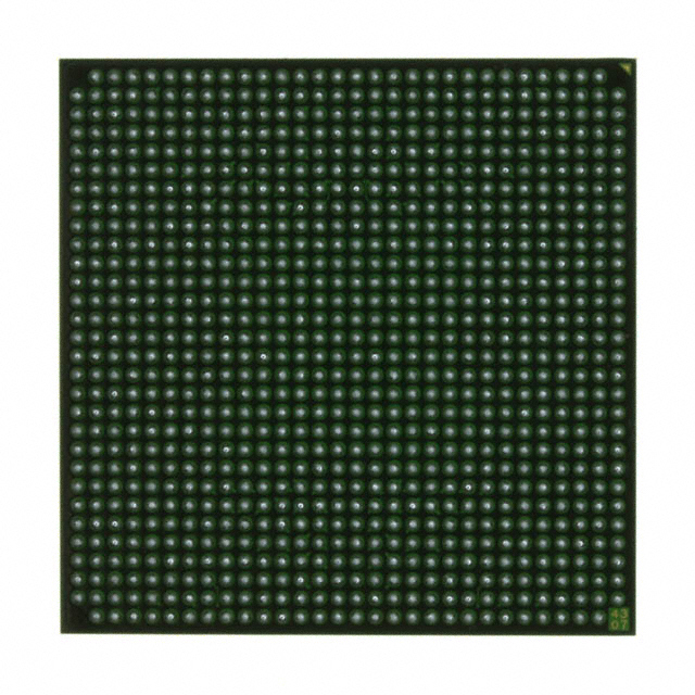
Virtex®-II Field Programmable Gate Array (FPGA) IC 392 884736 575-BBGA |
|---|---|
| Quantity | 261 Available (as of June 18, 2026) |

| Product Category | Field Programmable Gate Array (FPGA) |
|---|---|
| Manufacturer | AMD |
| Manufacturing Status | Obsolete |
| Manufacturer Standard Lead Time | Contact Us |
| Datasheet |
Specifications & Environmental
| Device Package | 575-BGA (31x31) | Grade | Commercial | Operating Temperature | 0°C – 85°C | ||
|---|---|---|---|---|---|---|---|
| Package / Case | 575-BBGA | Number of I/O | 392 | Voltage | 1.425 V - 1.575 V | ||
| Mounting Method | Surface Mount | RoHS Compliance | Unknown | REACH Compliance | REACH Unaffected | ||
| Moisture Sensitivity Level | 3 (168 Hours) | Number of LABs/CLBs | 1920 | Number of Logic Elements/Cells | 17280 | ||
| Number of Gates | 1500000 | ECCN | 3A991D | HTS Code | 8542.39.0001 | ||
| Qualification | N/A | Total RAM Bits | 884736 |
Overview of XC2V1500-4BGG575C – Virtex®-II Field Programmable Gate Array (FPGA) IC 392 884736 575-BBGA
The XC2V1500-4BGG575C is a Virtex®-II series field programmable gate array offering a high-capacity, reprogrammable logic fabric for complex digital designs. Built around the Virtex-II architecture, it combines a large number of logic elements, substantial embedded RAM, dedicated arithmetic blocks and extensive I/O to support memory interfaces, signal processing and custom logic functions.
This commercial-grade, surface-mount FPGA is optimized for designs requiring dense logic integration (approximately 17,280 logic elements and around 1.5 million system gates), on-chip memory (approximately 0.885 Mbits of embedded RAM) and a wide complement of I/O (392 pins) in a 575-BBGA package.
Key Features
- Core Logic Approximately 17,280 logic elements (1,920 CLBs) and roughly 1.5M gates provide large-scale programmable logic capacity for complex control, glue-logic and datapath implementations.
- Embedded Memory Approximately 0.885 Mbits of on-chip RAM (total RAM bits: 884,736) suitable for buffers, FIFOs and local data storage within your FPGA design.
- High I/O Count 392 user I/Os enable broad external interfacing for parallel buses, memory interfaces and multi-channel I/O requirements.
- Dedicated Arithmetic Resources Series documentation highlights dedicated 18-bit × 18-bit multiplier blocks and fast carry chains to accelerate arithmetic and DSP-oriented functions.
- Clock Management Virtex-II architecture includes Digital Clock Manager (DCM) resources for precise clock de-skew, frequency synthesis and phase control to support synchronous, multi-clock designs.
- Package & Mounting Supplied in a 575-BBGA (575-BGA, 31 × 31 mm) package for surface-mount PCB assembly, offering a dense footprint for high-pin-count applications.
- Electrical & Environmental Core supply voltage range of 1.425 V to 1.575 V and an operating temperature range of 0 °C to 85 °C; RoHS compliant and graded for commercial use.
Typical Applications
- Memory Interface Controllers Suitable for implementing high-performance SDR/DDR memory controllers and custom SRAM/DRAM interface logic leveraging the device’s large I/O count and on-chip RAM.
- Signal Processing and Acceleration Use the dedicated multiplier blocks and abundant logic resources to implement fixed-function accelerators, filters and arithmetic pipelines.
- High‑Density Logic Integration Ideal for consolidating multiple discrete components into a single programmable device for control, glue logic and complex state machines.
- Custom Prototyping and FPGA-Based Systems Well suited for board-level prototyping, proof-of-concept designs and deployable programmable systems that require substantial logic and memory resources.
Unique Advantages
- Large, Integrated Logic Fabric: Approximately 17,280 logic elements provide the capacity to implement sizeable digital systems within a single device, reducing BOM and board complexity.
- Significant On-Chip RAM: Approximately 0.885 Mbits of embedded memory supports local buffering and state storage for high-throughput data paths.
- Dedicated Arithmetic Blocks: Built-in 18 × 18 multipliers and fast carry logic accelerate DSP and math-heavy functions without consuming general-purpose logic.
- Flexible Clocking: On-chip DCM resources enable precise clock management for multi-clock and high-performance synchronous designs.
- High I/O Count in a Compact Package: 392 I/Os in a 575-BBGA footprint deliver wide connectivity while maintaining a compact PCB area.
- Commercial Grade and RoHS Compliant: Designed for commercial-temperature operation (0 °C to 85 °C) and compliant with RoHS requirements for regulatory alignment.
Why Choose XC2V1500-4BGG575C?
The XC2V1500-4BGG575C positions itself as a high-capacity Virtex‑II FPGA platform element for designers who need substantial logic, on-chip memory and arithmetic resources in a single, reprogrammable device. Its combination of approximately 17,280 logic elements, dedicated multiplier blocks and nearly 0.885 Mbits of embedded RAM supports demanding custom logic, memory interface and signal-processing tasks while simplifying system design.
Engineers building memory controllers, DSP accelerators, FPGA-based prototypes or consolidated digital systems will find this device offers a balanced mix of integration, I/O density and clock-management capability for scalable, manufacturable designs supported by Virtex‑II series documentation.
Request a quote or submit a procurement inquiry to obtain pricing, availability and lead-time information for the XC2V1500-4BGG575C.


Date Founded: 1969
Headquarters: Santa Clara, California, USA
Employees: 25,000+
Revenue: $22.68 Billion
Certifications and Memberships: ISO9001:2015, RoHS, REACH


