
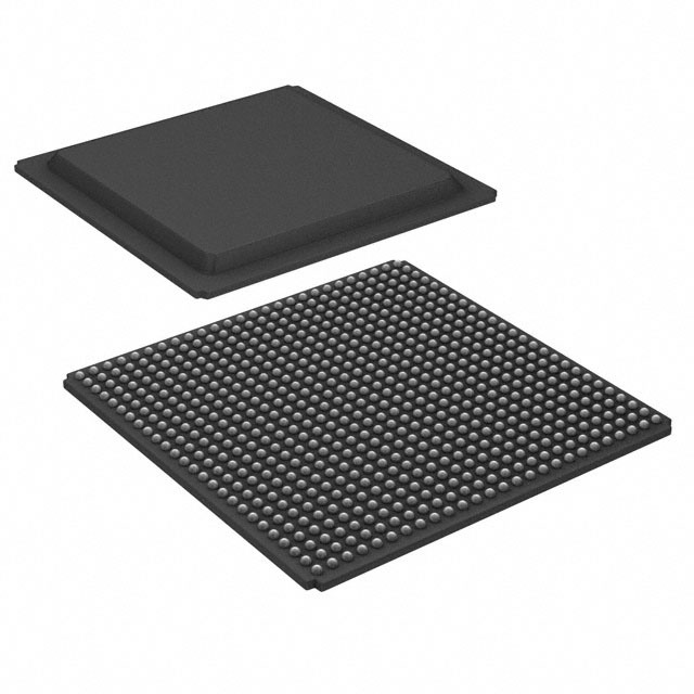
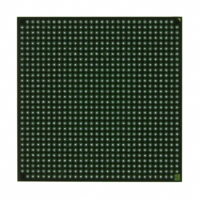
XC2V2000-4BGG575C
| Part Description |
Virtex®-II Field Programmable Gate Array (FPGA) IC 408 1032192 575-BBGA |
|---|---|
| Quantity | 1,804 Available (as of June 15, 2026) |

| Product Category | Field Programmable Gate Array (FPGA) |
|---|---|
| Manufacturer | AMD |
| Manufacturing Status | Obsolete |
| Manufacturer Standard Lead Time | Contact Us |
| Datasheet |
Specifications & Environmental
| Device Package | 575-BGA (31x31) | Grade | Commercial | Operating Temperature | 0°C – 85°C | ||
|---|---|---|---|---|---|---|---|
| Package / Case | 575-BBGA | Number of I/O | 408 | Voltage | 1.425 V - 1.575 V | ||
| Mounting Method | Surface Mount | RoHS Compliance | Unknown | REACH Compliance | REACH Unaffected | ||
| Moisture Sensitivity Level | 3 (168 Hours) | Number of LABs/CLBs | 2688 | Number of Logic Elements/Cells | 24192 | ||
| Number of Gates | 2000000 | ECCN | 3A991D | HTS Code | 8542.39.0001 | ||
| Qualification | N/A | Total RAM Bits | 1032192 |
Overview of XC2V2000-4BGG575C – Virtex®-II Field Programmable Gate Array (FPGA) IC 408 1032192 575-BBGA
The XC2V2000-4BGG575C is a Virtex®-II platform FPGA designed for high-density, configurable digital logic. Built on a platform architecture that includes block RAM resources, dedicated multipliers and clock-management functions, this device targets applications that require custom logic, embedded memory and high pin-count I/O integration.
This part provides 24,192 logic elements, approximately 1.03 Mbits of embedded memory and 408 user I/Os in a 575-ball BGA (31 × 31) package, making it suitable for complex system designs that need configurable hardware resources within a commercial temperature range.
Key Features
- Core logic capacity — 24,192 logic elements provide substantial programmable logic resources for implementing custom digital functions and glue logic.
- Configurable logic blocks — The device architecture includes CLB-based logic structures supporting lookup tables and registers for flexible logic implementation.
- Embedded memory — Total on-chip RAM of 1,032,192 bits (approximately 1.03 Mbits) for frame buffers, FIFOs and state storage.
- Dedicated arithmetic — Series architecture includes dedicated 18-bit × 18-bit multiplier resources for efficient hardware arithmetic and DSP tasks.
- I/O density and standards — 408 user I/Os available in a 575-BBGA package, enabling broad external interfacing options and high pin-count designs.
- Clock management — Platform-level clock management features such as Digital Clock Manager (DCM) modules support precise clocking and phase/frequency control.
- Package and mounting — 575-BBGA (575-BGA, 31 × 31) surface-mount package for high-density PCB integration.
- Power and operating range — Core supply voltage range of 1.425 V to 1.575 V; commercial operating temperature range 0 °C to 85 °C.
- Compliance — RoHS compliant for reduced environmental impact.
Typical Applications
- High-throughput interfaces — Implement DRAM/SRAM interface logic, buffering and protocol glue thanks to abundant I/O and embedded memory.
- Signal processing and DSP — Use built-in multiplier resources and dense logic to accelerate arithmetic-heavy pipelines and custom processing cores.
- Prototyping and system integration — Consolidate multiple glue and control functions into a single FPGA for platform development and system-level prototyping.
Unique Advantages
- Substantial programmable resources: 24,192 logic elements enable complex state machines, custom accelerators and large glue-logic implementations without external ASICs.
- On-chip memory for real workloads: Approximately 1.03 Mbits of embedded RAM supports buffering, FIFOs and mapped data structures, reducing external memory dependence.
- High I/O count in a compact BGA: 408 I/Os in a 575-ball BGA provide dense external connectivity while keeping board area efficient.
- Designed for precision clocking: Integrated clock-management features (DCMs) help maintain timing integrity across multiple high-speed domains.
- Commercial-grade readiness: Rated for 0 °C to 85 °C operation and RoHS compliant for standard commercial deployments.
Why Choose XC2V2000-4BGG575C?
The XC2V2000-4BGG575C delivers a balanced combination of logic capacity, embedded memory and I/O density in a single Virtex®-II FPGA package. Its on-chip resources and clock management capabilities let designers implement high-performance, application-specific hardware functions while minimizing external components.
This device is well suited for engineers building complex digital systems that require flexible, reprogrammable hardware—such as data path acceleration, protocol bridging and memory interface logic—within a commercial temperature range and RoHS-compliant supply chain.
Request a quote or submit an inquiry for pricing and availability to move your design forward with the XC2V2000-4BGG575C.


Date Founded: 1969
Headquarters: Santa Clara, California, USA
Employees: 25,000+
Revenue: $22.68 Billion
Certifications and Memberships: ISO9001:2015, RoHS, REACH


