
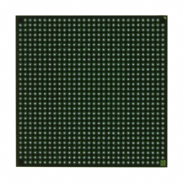
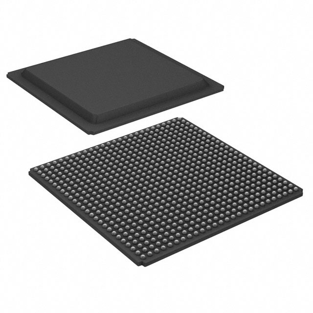
XC2V2000-4FFG896C
| Part Description |
Virtex®-II Field Programmable Gate Array (FPGA) IC 624 1032192 896-BBGA, FCBGA |
|---|---|
| Quantity | 1,002 Available (as of June 14, 2026) |
| Product Category | Field Programmable Gate Array (FPGA) |
|---|---|
| Manufacturer | AMD |
| Manufacturing Status | Obsolete |
| Manufacturer Standard Lead Time | Contact Us |
| Datasheet |
Specifications & Environmental
| Device Package | 896-FCBGA (31x31) | Grade | Commercial | Operating Temperature | 0°C – 85°C | ||
|---|---|---|---|---|---|---|---|
| Package / Case | 896-BBGA, FCBGA | Number of I/O | 624 | Voltage | 1.425 V - 1.575 V | ||
| Mounting Method | Surface Mount | RoHS Compliance | Unknown | REACH Compliance | REACH Unaffected | ||
| Moisture Sensitivity Level | 4 (72 Hours) | Number of LABs/CLBs | 2688 | Number of Logic Elements/Cells | 24192 | ||
| Number of Gates | 2000000 | ECCN | 3A001A7A | HTS Code | 8542.39.0001 | ||
| Qualification | N/A | Total RAM Bits | 1032192 |
Overview of XC2V2000-4FFG896C – Virtex®-II FPGA IC, 896-FCBGA, 624 I/O
The XC2V2000-4FFG896C from AMD is a Virtex®-II field programmable gate array supplied in a 896-FCBGA (31×31) package. This commercial-grade FPGA delivers high integration for logic-intensive designs, offering 24,192 logic elements, approximately 1.03 Mbits of embedded memory, and 624 user I/Os.
Built on the Virtex-II platform architecture, the device supports SelectRAM memory hierarchy, dedicated multiplier blocks and advanced clock-management features suitable for designs requiring flexible memory interfaces, arithmetic acceleration and complex I/O routing.
Key Features
- Core Logic 24,192 logic elements and an estimated 2,000,000 system gates provide programmable fabric for complex digital designs.
- Embedded Memory Approximately 1.03 Mbits of on-chip RAM (1,032,192 total RAM bits) combined with the series SelectRAM block architecture for local and block RAM usage.
- Arithmetic Resources Series-level support for dedicated 18‑bit × 18‑bit multipliers enables high-throughput arithmetic and DSP functions.
- Clock Management Virtex‑II platform features include Digital Clock Manager (DCM) modules and global clock multiplexer buffers to support precise clock de‑skew and flexible frequency handling.
- High-Density I/O 624 user I/O pins with SelectIO capabilities; series features include multiple I/O standards, Digitally Controlled Impedance (DCI) and programmable sink current options.
- Package & Mounting 896‑BBGA (FCBGA) surface-mount package, supplier device package listed as 896‑FCBGA (31×31), suitable for compact board-level integration.
- Power & Temperature Core supply range 1.425 V to 1.575 V; commercial operating temperature 0 °C to 85 °C.
- Compliance RoHS compliant.
Typical Applications
- Memory Interface Controllers Use the device’s SelectRAM architecture and series DRAM/SRAM interface support to implement custom memory controllers and high-performance bridging logic.
- Signal Processing / DSP Dedicated 18×18 multipliers and substantial logic capacity enable arithmetic acceleration, filtering and medium-scale DSP pipelines.
- High‑Density I/O Systems With 624 I/Os and SelectIO features, deploy the device for multi-protocol I/O aggregation, protocol bridging and complex board I/O functions.
- Prototyping and Embedded Systems The combination of logic density, embedded RAM and clock management makes it suitable for prototype platforms and embedded digital controllers.
Unique Advantages
- High logic capacity: 24,192 logic elements enable consolidation of multiple functions into a single device, reducing system BOM.
- On‑chip memory availability: Approximately 1.03 Mbits of embedded RAM supports local buffering and state storage without immediate external memory.
- Rich I/O resources: 624 user I/Os provide extensive interfacing options for dense connector and board-level designs.
- Targeted arithmetic support: Dedicated 18×18 multipliers accelerate compute-heavy tasks and simplify DSP implementation.
- Compact package: 896‑FCBGA (31×31) surface-mount package balances high pin count with a small PCB footprint for space-constrained boards.
- Regulated supply and commercial grade: Defined core voltage range (1.425 V–1.575 V) and 0 °C–85 °C rating simplify power and thermal planning for commercial applications.
Why Choose XC2V2000-4FFG896C?
The XC2V2000-4FFG896C positions itself as a versatile, high‑integration Virtex‑II FPGA suitable for designers needing substantial logic, embedded memory and extensive I/O in a compact FCBGA package. Its platform-level features—such as SelectRAM memory hierarchy, multiplier blocks and clock management—deliver the building blocks required for custom memory interfaces, DSP acceleration and complex I/O tasks.
This device is appropriate for development and production in commercial temperature environments where on-chip resources and flexible I/O reduce board complexity and accelerate time-to-market. RoHS compliance and defined electrical/thermal parameters support predictable integration into commercial systems.
Request a quote or submit an inquiry to receive pricing and availability information for the XC2V2000-4FFG896C.


Date Founded: 1969
Headquarters: Santa Clara, California, USA
Employees: 25,000+
Revenue: $22.68 Billion
Certifications and Memberships: ISO9001:2015, RoHS, REACH


