
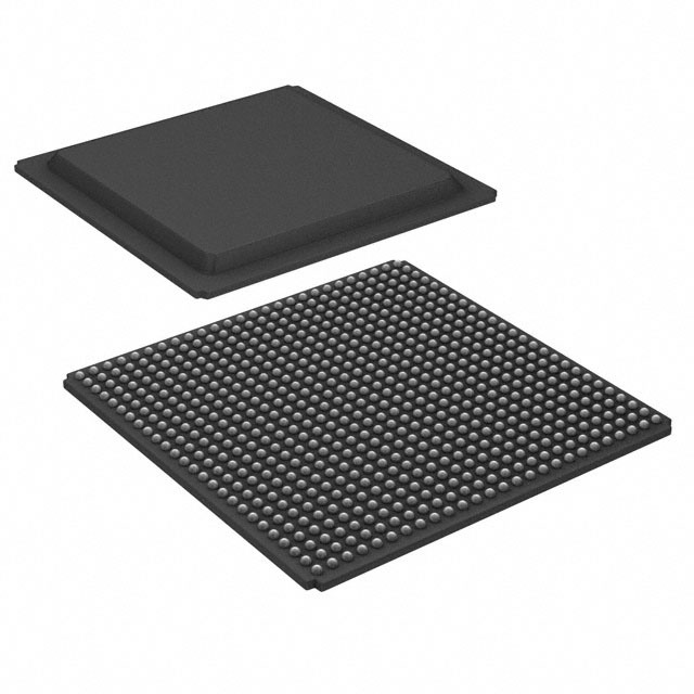
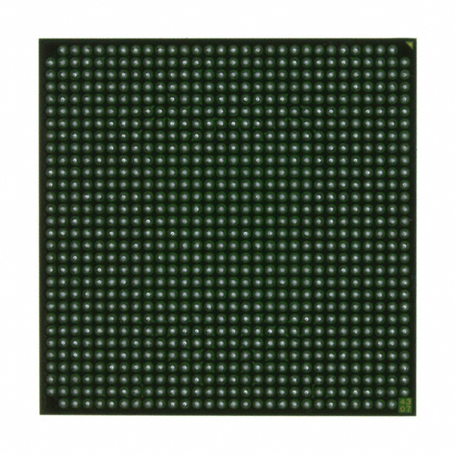
XC2V2000-4FGG676C
| Part Description |
Virtex®-II Field Programmable Gate Array (FPGA) IC 456 1032192 676-BGA |
|---|---|
| Quantity | 976 Available (as of June 15, 2026) |

| Product Category | Field Programmable Gate Array (FPGA) |
|---|---|
| Manufacturer | AMD |
| Manufacturing Status | Obsolete |
| Manufacturer Standard Lead Time | Contact Us |
| Datasheet |
Specifications & Environmental
| Device Package | 676-FBGA (27x27) | Grade | Commercial | Operating Temperature | 0°C – 85°C | ||
|---|---|---|---|---|---|---|---|
| Package / Case | 676-BGA | Number of I/O | 456 | Voltage | 1.425 V - 1.575 V | ||
| Mounting Method | Surface Mount | RoHS Compliance | Unknown | REACH Compliance | REACH Unaffected | ||
| Moisture Sensitivity Level | 3 (168 Hours) | Number of LABs/CLBs | 2688 | Number of Logic Elements/Cells | 24192 | ||
| Number of Gates | 2000000 | ECCN | 3A991D | HTS Code | 8542.39.0001 | ||
| Qualification | N/A | Total RAM Bits | 1032192 |
Overview of XC2V2000-4FGG676C – Virtex®-II FPGA, 676-BGA, Commercial
The XC2V2000-4FGG676C is a Virtex®-II field programmable gate array supplied in a 676-ball fine-pitch BGA package. It combines a large logic fabric with substantial on-chip RAM and a high pin-count I/O complement, making it suitable for demanding digital designs that require flexible, reprogrammable logic integration.
Built on the Virtex-II platform, this device targets applications that benefit from abundant logic resources, embedded memory, and a rich I/O set while operating within a commercial temperature range and a 1.425 V–1.575 V core supply window.
Key Features
- Logic Capacity: 24,192 logic elements (cells) provide substantial programmable logic for complex designs; the part lists approximately 2,000,000 system gates.
- Configurable Logic Blocks (CLBs): 2,688 CLBs (platform-defined resource) for implementing combinational and sequential logic structures.
- Embedded Memory: Approximately 1.03 Mbits of on-chip RAM (1,032,192 bits) via 18-Kb block SelectRAM resources for data buffering and state storage.
- High I/O Count: 456 user I/O pins for broad external connectivity in a wide range of system interfaces.
- Arithmetic Resources: Dedicated 18-bit × 18-bit multiplier blocks (Virtex®-II platform feature) for efficient fixed-point and DSP-style arithmetic.
- Clock Management: Digital Clock Manager (DCM) functionality (platform feature) including multiple DCM modules for deskewing, frequency synthesis, and phase shifting.
- Package and Mounting: 676-ball fine-pitch BGA (676-FBGA, 27 × 27 mm) in a surface-mount configuration for PCB integration.
- Power and Temperature: Core supply range of 1.425 V to 1.575 V and commercial operating temperature from 0 °C to 85 °C.
- Standards and Platform Capabilities: Virtex-II platform features include SelectRAM memory hierarchy, SelectIO™ options, and high-performance routing and interconnect (as described in the Virtex-II series specification).
- RoHS Compliance: Device is RoHS compliant.
Typical Applications
- Communications and Networking: Use the device’s large logic capacity, embedded RAM, and multiple I/Os for protocol processing, packet buffering, and custom interface bridging.
- Signal Processing and DSP: Leverage the dedicated 18-bit × 18-bit multipliers and on-chip RAM for fixed-point filtering, transforms, and acceleration of compute-heavy kernels.
- High-Density Digital Systems: Ideal for control logic, glue-logic consolidation, and custom datapaths where many I/Os and substantial programmable logic are required.
- Memory Interface and Controller Prototyping: Use the embedded RAM and platform memory hierarchy to implement DRAM/SRAM interface logic and buffering functions during development.
Unique Advantages
- Large, Flexible Logic Fabric: 24,192 logic elements and 2,688 CLBs allow complex finite-state machines, custom datapaths, and wide combinational logic to be implemented on-chip.
- Integrated On-Chip Memory: Approximately 1.03 Mbits of embedded RAM reduce external memory dependence and simplify board-level design for many buffering and storage tasks.
- Rich I/O Resources: 456 user I/Os provide design flexibility for interfacing multiple peripherals, external memories, and high-pin-count connectors without additional bridge components.
- Dedicated Arithmetic Blocks: On-chip 18 × 18 multipliers accelerate arithmetic operations and reduce the need for external DSP ASICs.
- Platform-Level Clock Management: Digital Clock Manager resources support precise clocking and phase control for synchronized, high-performance systems.
- Commercial Temperature and RoHS Compliance: Designed for commercial environments (0 °C to 85 °C) and RoHS-compliant manufacturing requirements.
Why Choose XC2V2000-4FGG676C?
The XC2V2000-4FGG676C delivers a balance of substantial programmable logic, embedded RAM, arithmetic resources, and a high I/O count in a 676-ball FBGA package. It is well suited to engineers building complex digital systems that require reprogrammability, on-chip memory, and extensive interfacing capabilities within commercial temperature ranges.
As part of the Virtex®-II platform, it aligns with platform-level features such as SelectRAM and DCM support, providing design scalability and a familiar development flow for FPGA-based system implementations.
Request a quote or submit an RFQ to get pricing and availability for the XC2V2000-4FGG676C and discuss quantity-based options or lead times.


Date Founded: 1969
Headquarters: Santa Clara, California, USA
Employees: 25,000+
Revenue: $22.68 Billion
Certifications and Memberships: ISO9001:2015, RoHS, REACH


