
XC2VP100-6FF1704I
| Part Description |
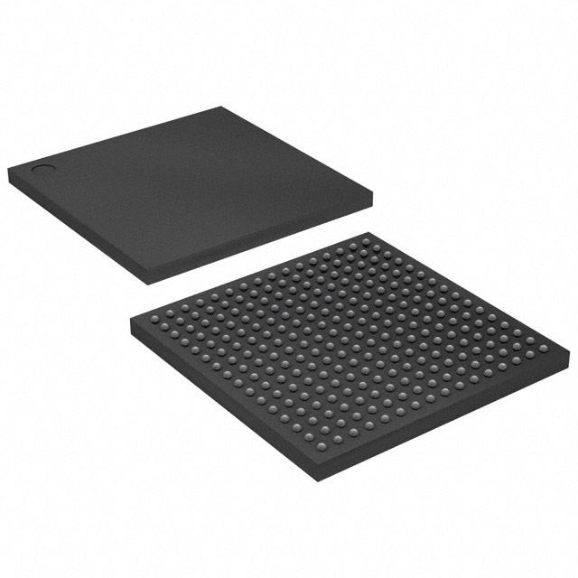
Virtex®-II Pro Field Programmable Gate Array (FPGA) IC 1040 8183808 99216 1704-BBGA, FCBGA |
|---|---|
| Quantity | 547 Available (as of June 15, 2026) |

| Product Category | Field Programmable Gate Array (FPGA) |
|---|---|
| Manufacturer | AMD |
| Manufacturing Status | Obsolete |
| Manufacturer Standard Lead Time | Contact Us |
| Datasheet |
Specifications & Environmental
| Device Package | 1704-FCBGA (42.5x42.5) | Grade | Industrial | Operating Temperature | -40°C – 100°C | ||
|---|---|---|---|---|---|---|---|
| Package / Case | 1704-BBGA, FCBGA | Number of I/O | 1040 | Voltage | 1.425 V - 1.575 V | ||
| Mounting Method | Surface Mount | RoHS Compliance | RoHS non-compliant | REACH Compliance | REACH Unaffected | ||
| Moisture Sensitivity Level | 4 (72 Hours) | Number of LABs/CLBs | 11024 | Number of Logic Elements/Cells | 99216 | ||
| Number of Gates | N/A | ECCN | 3A001A7A | HTS Code | 8542.39.0001 | ||
| Qualification | N/A | Total RAM Bits | 8183808 |
Overview of XC2VP100-6FF1704I – Virtex®-II Pro Field Programmable Gate Array, 1704-FCBGA (Industrial)
The XC2VP100-6FF1704I is a Virtex®-II Pro FPGA in a 1704-FCBGA package (42.5 × 42.5 mm) designed for high-density, high-I/O applications. This SRAM-based platform device integrates large programmable logic capacity, multi-gigabit transceiver support and embedded processor resources to address complex system designs.
With 99,216 logic elements, approximately 8.18 Mbits of embedded memory and 1,040 user I/O pins, the device targets applications requiring substantial logic, memory and I/O integration while supporting industrial operating temperatures and standard surface-mount assembly.
Key Features
- High Logic Density — 99,216 logic elements to implement large, complex designs and custom logic functions.
- Embedded Memory — Approximately 8.18 Mbits of on-chip RAM for buffers, FIFOs and local storage.
- Extensive I/O — 1,040 user I/O pins to support wide data buses, parallel interfaces and heterogeneous signal routing.
- Embedded Processor Blocks — Device family support for up to two IBM PowerPC™ RISC processor blocks for on-chip processing and control integration.
- Multi-Gigabit Transceivers — Support for RocketIO™ and RocketIO X high-speed serial transceivers, including telecom/datacom support modes and programmable output swing and pre-emphasis.
- Dedicated DSP Resources — On-chip 18-bit × 18-bit multiplier blocks for efficient implementation of signal-processing and math-intensive functions.
- Clock and Timing — Integrated digital clock management and global clock multiplexing for flexible, high-performance clock distribution.
- Selectable I/O Technologies — SelectI/O™-Ultra and Digitally Controlled Impedance (DCI) features to simplify interface tuning and signal integrity management.
- Package & Mounting — 1704-FCBGA (1704-BBGA) surface-mount package, 42.5 × 42.5 mm, suitable for high-pin-count board designs.
- Power & Temperature — Core supply range 1.425 V to 1.575 V and industrial operating range from −40 °C to 100 °C.
- Compliance — RoHS compliant.
Typical Applications
- Telecom & Datacom Systems — High-speed RocketIO transceivers and telecom/datacom support modes enable implementation of serial links and protocol interfaces.
- Embedded Processing Platforms — On-chip PowerPC processor blocks allow integration of control and data-path processing within the FPGA fabric.
- High-Density Logic and Memory Systems — Large logic element count and approximately 8.18 Mbits of embedded RAM support complex state machines, packet buffering and custom accelerators.
- High-Pin-Count I/O Designs — 1,040 I/O pins facilitate wide parallel buses, multi-interface boards and extensive external device connectivity.
Unique Advantages
- Highly Integrated Platform: Combines substantial programmable logic, on-chip memory and embedded processor capability to reduce external component count and system complexity.
- Multi-Gigabit SerDes Support: RocketIO transceivers with programmable swing and pre-emphasis simplify design of high-speed serial links and telecom interfaces.
- Dedicated DSP Resources: 18×18 multipliers accelerate arithmetic and signal-processing functions without consuming general logic resources.
- Robust I/O and Clocking: Large I/O count plus digital clock management and SelectI/O technologies enable flexible interface design and reliable timing across the system.
- Industrial Temperature Range: Rated from −40 °C to 100 °C for deployment in temperature-challenging environments.
- Standard Surface-Mount Package: 1704-FCBGA format supports dense PCB integration for complex, space-constrained systems.
Why Choose XC2VP100-6FF1704I?
The XC2VP100-6FF1704I positions itself as a high-density, feature-rich Virtex®-II Pro FPGA suitable for systems that require extensive logic, embedded memory and large I/O capability combined with on-chip processing and high-speed serial connectivity. Its combination of approximately 8.18 Mbits of embedded RAM, 99,216 logic elements, RocketIO transceiver support and PowerPC processor integration makes it well suited to demanding telecom, datacom and embedded processing applications that benefit from tight integration and reduced board-level complexity.
With industrial temperature rating, RoHS compliance and a high-pin-count FCBGA package, the part supports professional engineering designs where integration density, I/O bandwidth and on-chip processing are key selection criteria.
Request a quote or submit an inquiry to receive pricing and availability for the XC2VP100-6FF1704I and to discuss how this Virtex®-II Pro FPGA can fit into your next design.


Date Founded: 1969
Headquarters: Santa Clara, California, USA
Employees: 25,000+
Revenue: $22.68 Billion
Certifications and Memberships: ISO9001:2015, RoHS, REACH


