
XC2VP100-6FFG1704I
| Part Description |
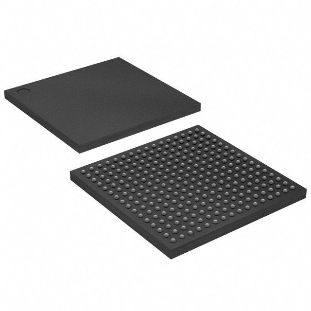
Virtex®-II Pro Field Programmable Gate Array (FPGA) IC 1040 8183808 99216 1704-BBGA, FCBGA |
|---|---|
| Quantity | 1,003 Available (as of June 15, 2026) |

| Product Category | Field Programmable Gate Array (FPGA) |
|---|---|
| Manufacturer | AMD |
| Manufacturing Status | Obsolete |
| Manufacturer Standard Lead Time | Contact Us |
| Datasheet |
Specifications & Environmental
| Device Package | 1704-FCBGA (42.5x42.5) | Grade | Industrial | Operating Temperature | -40°C – 100°C | ||
|---|---|---|---|---|---|---|---|
| Package / Case | 1704-BBGA, FCBGA | Number of I/O | 1040 | Voltage | 1.425 V - 1.575 V | ||
| Mounting Method | Surface Mount | RoHS Compliance | ROHS3 Compliant | REACH Compliance | REACH Unaffected | ||
| Moisture Sensitivity Level | 4 (72 Hours) | Number of LABs/CLBs | 11024 | Number of Logic Elements/Cells | 99216 | ||
| Number of Gates | N/A | ECCN | 3A001A7A | HTS Code | 8542.39.0001 | ||
| Qualification | N/A | Total RAM Bits | 8183808 |
Overview of XC2VP100-6FFG1704I – Virtex®-II Pro FPGA, 1704-FCBGA, Industrial
The XC2VP100-6FFG1704I is a Virtex®-II Pro family field programmable gate array offered in a 1704-ball FCBGA package. It delivers a high-capacity, platform-class FPGA architecture designed for applications that require large logic density, extensive I/O, and substantial on-chip memory.
Built for industrial environments, this device combines configurable logic resources with the Virtex-II Pro family feature set—including high-speed serial transceiver options and embedded processor block support—providing integration and flexibility for communications, embedded processing, and system-level designs.
Key Features
- Logic Capacity 99,216 logic cells and 11,024 CLBs provide substantial programmable fabric for complex SoC and high-density logic implementations.
- Embedded Memory Approximately 8.18 Mbits of embedded RAM to support large buffering, packet processing, and on-chip data storage.
- High I/O Count Up to 1,040 I/O pins accommodate wide parallel interfaces and multiple high-speed external connections.
- Virtex-II Pro Family Capabilities Family features include support for RocketIO multi-gigabit transceivers and up to two PowerPC™ 405 processor blocks, plus SelectRAM+ memory hierarchy and dedicated 18×18 multiplier blocks for DSP tasks.
- Clocking and Timing Integrated clock management features such as Digital Clock Manager (DCM) elements enable flexible and high-performance clocking architectures.
- Package and Mounting 1704-FCBGA package (42.5 × 42.5 mm) in a surface-mount form factor for high-density board designs.
- Power and Temperature Core supply range of 1.425 V to 1.575 V and an operating temperature range of −40 °C to 100 °C suited to industrial temperature conditions.
- Compliance RoHS-compliant construction for environmental and regulatory considerations.
Typical Applications
- Telecom & Datacom Systems Use the family’s RocketIO multi-gigabit transceiver support and large I/O count for high-bandwidth networking, line cards, and protocol bridging.
- Embedded Processing Platforms Integrate on-chip PowerPC processor blocks and programmable logic to implement control planes, protocol stacks, and custom accelerators.
- Signal Processing & DSP Leverage dedicated 18×18 multipliers and abundant embedded RAM for filtering, encoding/decoding, and other high-throughput DSP tasks.
- System Prototyping & Integration Large logic capacity and extensive I/O make the device suitable for system integration, custom SoC prototyping, and complex FPGA-based subsystems.
Unique Advantages
- High Integration Density: Nearly 100k logic cells and 11k CLBs reduce external components by enabling large portions of system logic on-chip.
- Substantial On-Chip Memory: Approximately 8.18 Mbits of embedded RAM supports deep buffering and data-path storage without relying on external memory.
- Extensive I/O Capability: 1,040 I/Os provide flexibility for wide buses, multiple peripherals, and parallel interfaces across complex designs.
- Industrial Temperature Range: Rated from −40 °C to 100 °C for deployment in industrial environments where extended operating range is required.
- Robust Packaging: The 1704-FCBGA (42.5 × 42.5 mm) package supports high pin-count, high-density board layouts for advanced system designs.
- Standards-Conscious Manufacturing: RoHS compliance aligns with modern production and regulatory requirements.
Why Choose XC2VP100-6FFG1704I?
The XC2VP100-6FFG1704I positions itself as a platform-class FPGA option for engineers who need substantial logic resources, large embedded memory, and broad I/O in an industrial-grade package. Its Virtex-II Pro family capabilities—such as support for multi-gigabit transceivers and embedded processor blocks—enable highly integrated designs that consolidate functions and reduce BOM complexity.
This device is well suited for teams developing communications equipment, embedded processing platforms, and high-throughput DSP systems that require deterministic temperature and power specifications, long-term documentation, and a field-programmable integration path for system updates and iteration.
If you would like pricing, availability, or to request a formal quote for the XC2VP100-6FFG1704I, submit a quote request or product inquiry and our team will respond with the next steps.


Date Founded: 1969
Headquarters: Santa Clara, California, USA
Employees: 25,000+
Revenue: $22.68 Billion
Certifications and Memberships: ISO9001:2015, RoHS, REACH


