
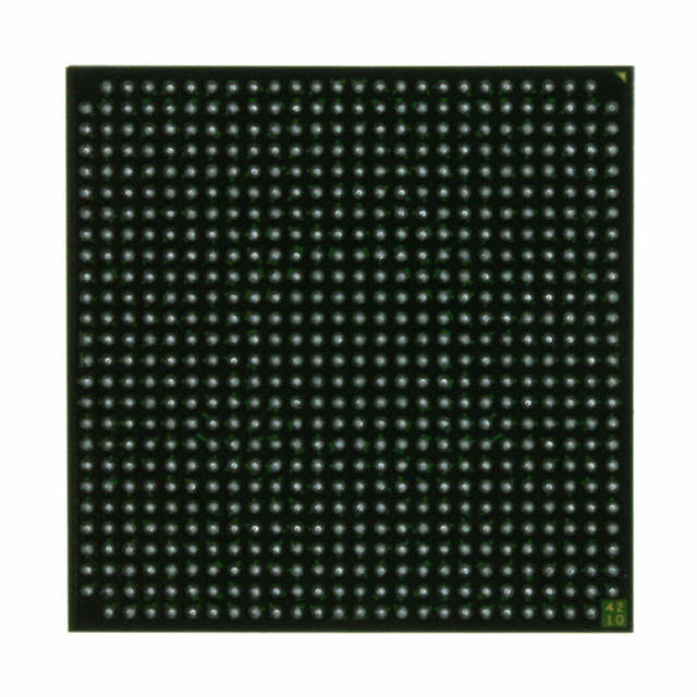
XC2VP7-5FF672C
| Part Description |
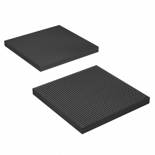
Virtex®-II Pro Field Programmable Gate Array (FPGA) IC 396 811008 11088 672-BBGA, FCBGA |
|---|---|
| Quantity | 952 Available (as of October 8, 2026) |
| Product Category | Field Programmable Gate Array (FPGA) |
|---|---|
| Manufacturer | AMD |
| Manufacturing Status | Obsolete |
| Manufacturer Standard Lead Time | Contact Us |
| Datasheet |
Specifications & Environmental
| Device Package | 672-FCBGA (27x27) | Grade | Commercial | Operating Temperature | 0°C – 85°C | ||
|---|---|---|---|---|---|---|---|
| Package / Case | 672-BBGA, FCBGA | Number of I/O | 396 | Voltage | 1.425 V - 1.575 V | ||
| Mounting Method | Surface Mount | RoHS Compliance | RoHS non-compliant | REACH Compliance | REACH Unaffected | ||
| Moisture Sensitivity Level | 4 (72 Hours) | Number of LABs/CLBs | 1232 | Number of Logic Elements/Cells | 11088 | ||
| Number of Gates | N/A | ECCN | 3A991D | HTS Code | 8542.39.0001 | ||
| Qualification | N/A | Total RAM Bits | 811008 |
Overview of XC2VP7-5FF672C – Virtex®-II Pro Field Programmable Gate Array (FPGA) IC
The XC2VP7-5FF672C is a commercial-grade Virtex®-II Pro platform FPGA from AMD, offered in a 672-ball flip-chip BGA (672-FCBGA, 27×27) package for surface-mount applications. The device exposes a high pin-count I/O set and a balanced mix of logic, embedded memory, and platform-level features suitable for embedded processing and high‑performance I/O applications.
Device-level specifications include a nominal core supply range and commercial operating temperature, while the Virtex‑II Pro family provides platform features such as embedded processor blocks, multi‑gigabit transceiver support, and a rich set of on-chip resources described in the Virtex‑II Pro documentation.
Key Features
- Logic Capacity — 1,232 CLBs supporting 11,088 logic elements, enabling complex custom logic and control functions.
- Embedded Memory — Approximately 0.81 Mbits (811,008 bits) of on-chip RAM for buffering, LUT-based storage, and local data structures.
- I/O — 396 dedicated I/O pins to support wide parallel interfaces and diverse external connections.
- Package & Mounting — 672‑BBGA (672‑FCBGA, 27×27) flip‑chip BGA package, surface mount.
- Power Supply — Core voltage specified from 1.425 V to 1.575 V for precise power budgeting.
- Operating Range & Grade — Commercial grade device rated for 0 °C to 85 °C operation; RoHS compliant.
- Virtex‑II Pro Platform Features — Family-level capabilities documented for Virtex‑II Pro include embedded multi‑gigabit transceivers (RocketIO™/RocketIO X), up to two embedded PowerPC™ 405 processor blocks, SelectRAM™ memory hierarchy, dedicated 18×18 multipliers, digital clock management (DCM), and Digitally Controlled Impedance (DCI) I/O technologies.
- Design & Reference Support — Platform documentation includes IP core and reference support to aid integration and system design (see Virtex‑II Pro documentation for details).
Typical Applications
- Embedded Processing — Integration of custom logic with on‑chip memory and the Virtex‑II Pro platform’s processor resources for system control and pre/post processing tasks.
- High‑Pin‑Count Interface Control — Implement wide parallel interfaces, protocol bridges, or aggregation logic using 396 I/Os.
- High‑Performance DSP and Acceleration — Use the device’s logic elements, embedded RAM, and 18×18 multipliers for signal processing pipelines and hardware acceleration.
- Connectivity and Multi‑Gigabit Front Ends — Architect multi‑gigabit or high‑speed serial subsystems leveraging the Virtex‑II Pro family’s transceiver and I/O capabilities (refer to family documentation for transceiver availability and configuration).
Unique Advantages
- Balanced Resource Mix: Combines 11,088 logic elements with approximately 0.81 Mbits of embedded RAM for control, buffering, and data‑path implementations without external memory in many use cases.
- High I/O Density: 396 I/O pins provide flexibility for interfacing to peripherals, external memories, and wide buses, reducing the need for external muxing or interface chips.
- Compact BGA Package: 672‑FBGA (27×27) flip‑chip package saves PCB area while delivering high pin count for complex system designs.
- Platform-Level Capability: Access to Virtex‑II Pro family features—documented processor blocks, transceiver technology, and clocking resources—helps accelerate system-level design and IP reuse.
- Commercial Temperature & RoHS Compliance: Rated for 0 °C to 85 °C operation and RoHS compliant for standard commercial deployments.
- Precise Power Specification: Defined core voltage window (1.425 V to 1.575 V) simplifies power-supply design and margining for production systems.
Why Choose XC2VP7-5FF672C?
The XC2VP7-5FF672C positions itself as a Virtex‑II Pro platform FPGA that blends mid‑range logic capacity, substantial embedded memory, and a high I/O count in a compact flip‑chip BGA package. It is well suited to designers building embedded systems, interface controllers, and DSP-accelerated subsystems that require a balance of logic, memory, and connectivity within commercial temperature constraints.
Backed by Virtex‑II Pro platform documentation and IP/processor references, the device provides documented architecture and system resources that help reduce integration time and support scalable designs across the Virtex‑II Pro family.
Request a quote or submit an inquiry to check availability, lead time, and pricing for the XC2VP7-5FF672C.
























Date Founded: 1969
Headquarters: Santa Clara, California, USA
Employees: 25,000+
Revenue: $22.68 Billion
Certifications and Memberships: ISO9001:2015, RoHS, REACH











