
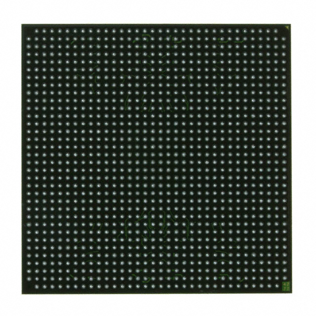
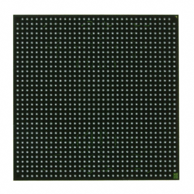
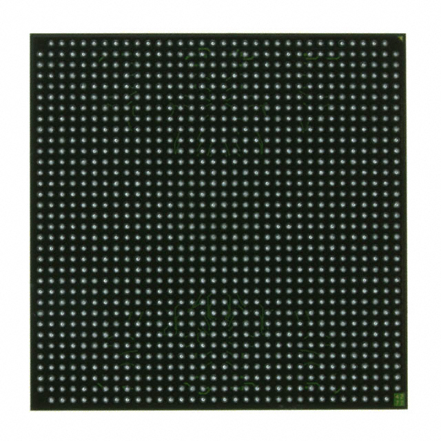
XC2VP50-6FFG1152I
| Part Description |
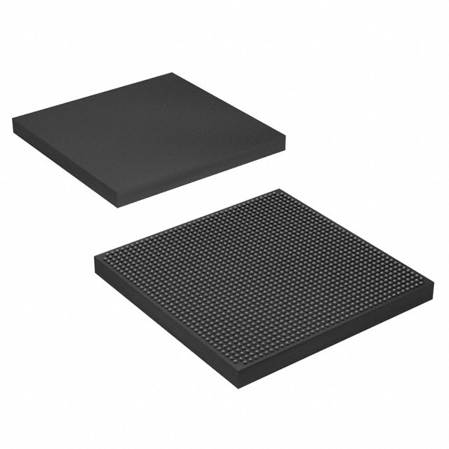
Virtex®-II Pro Field Programmable Gate Array (FPGA) IC 692 4276224 53136 1152-BBGA, FCBGA |
|---|---|
| Quantity | 663 Available (as of October 7, 2026) |
| Product Category | Field Programmable Gate Array (FPGA) |
|---|---|
| Manufacturer | AMD |
| Manufacturing Status | Obsolete |
| Manufacturer Standard Lead Time | Contact Us |
| Datasheet |
Specifications & Environmental
| Device Package | 1152-FCBGA (35x35) | Grade | Industrial | Operating Temperature | -40°C – 100°C | ||
|---|---|---|---|---|---|---|---|
| Package / Case | 1152-BBGA, FCBGA | Number of I/O | 692 | Voltage | 1.425 V - 1.575 V | ||
| Mounting Method | Surface Mount | RoHS Compliance | ROHS3 Compliant | REACH Compliance | REACH Unaffected | ||
| Moisture Sensitivity Level | 4 (72 Hours) | Number of LABs/CLBs | 5904 | Number of Logic Elements/Cells | 53136 | ||
| Number of Gates | N/A | ECCN | 3A001A7A | HTS Code | 8542.39.0001 | ||
| Qualification | N/A | Total RAM Bits | 4276224 |
Overview of XC2VP50-6FFG1152I – Virtex®-II Pro Field Programmable Gate Array (FPGA) IC 692 I/O, ~4.28 Mbits RAM, 53136 logic elements, 1152-FCBGA
The XC2VP50-6FFG1152I is a Virtex®-II Pro platform FPGA provided in a 1152‑ball FCBGA package. This SRAM-based FPGA integrates a large logic fabric and embedded memory, delivering a flexible, reprogrammable platform for embedded-processing and high-density I/O applications.
Designed for industrial-grade deployments, the device offers substantial logic resources, a high I/O count and support for the Virtex‑II Pro family features such as on-chip processor blocks and multi-gigabit transceiver capabilities described in the product specification.
Key Features
- Logic Capacity: 53136 logic elements to implement complex combinational and sequential logic.
- Embedded Memory: Approximately 4.28 Mbits of on-chip RAM for buffering, state storage and memory-intensive logic.
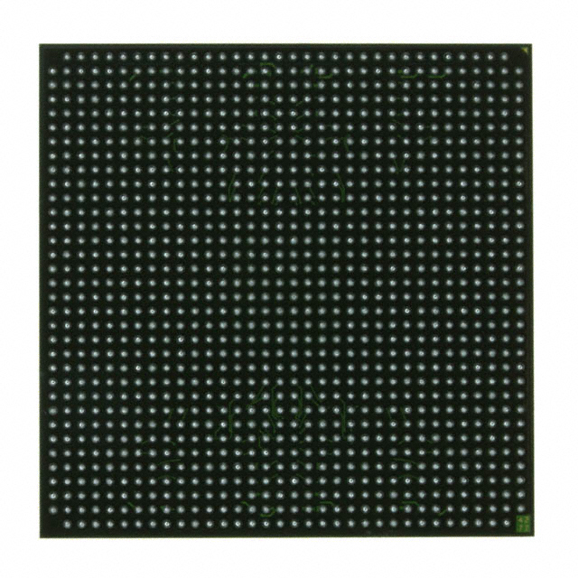
- I/O Density & Package: 692 user I/O pins in a 1152‑ball FCBGA (35×35) package, supporting high interface density in a single surface-mount footprint.
- Platform Architecture: Virtex‑II Pro family architecture with platform-level features including configurable logic blocks, SelectRAM memory hierarchy, and advanced clock management as outlined in the product specification.
- On-Chip Processing & Transceivers: Family-level support for embedded PowerPC™ 405 processor blocks and RocketIO multi-gigabit transceivers (family capabilities described in the datasheet).
- Power Supply Range: Core supply range of 1.425 V to 1.575 V for defined operating conditions.
- Industrial Temperature Rating: Specified operating range from −40 °C to 100 °C for industrial applications.
- Compliance: RoHS compliant.
Typical Applications
- Telecom / Datacom Systems: High I/O count and family support for RocketIO transceivers enable deployments that require dense serial interfaces and telecom/datacom protocols.
- Embedded Processing Platforms: On-chip PowerPC processor block support and abundant logic/memory make the device suitable for embedded controller and system-on-chip style implementations.
- High‑Bandwidth Interface Hubs: Large logic capacity and substantial on-chip RAM support data buffering, protocol bridging and complex interface aggregation.
- Industrial Control & Automation: Industrial temperature rating and robust I/O count allow use in control systems that require extended temperature operation and extensive sensor/actuator connectivity.
Unique Advantages
- Substantial Logic Resources: 53136 logic elements provide headroom for complex algorithms, signal processing and control logic without external ASICs.
- Significant Embedded Memory: Approximately 4.28 Mbits of on-chip RAM reduces reliance on external memory for many buffering and stateful tasks.
- High I/O Count in a Compact Package: 692 I/Os in a 1152‑ball FCBGA (35×35) delivers a high interface density in a surface-mount package suitable for compact board layouts.
- Industrial Temperature Range: Rated from −40 °C to 100 °C for reliable operation in industrial environments.
- Platform-Level Integration: Virtex‑II Pro family features such as embedded processor blocks and multi-gigabit transceiver support provide integration options that can reduce external components and BOM complexity.
- RoHS Compliant: Conforms to RoHS requirements for environmentally conscious designs.
Why Choose XC2VP50-6FFG1152I?
The XC2VP50-6FFG1152I combines a high logic count, substantial on-chip memory and a very high I/O density in a single industrial‑rated FCBGA package. Its Virtex‑II Pro platform heritage brings family-level features—embedded processor blocks, multi-gigabit transceiver support and advanced clocking—that help simplify system design and integration for embedded and telecom applications.
This device is well suited to designers needing a flexible, reprogrammable platform with robust logic and memory resources, dense interfacing and industrial temperature capability. It is a practical choice for applications where consolidation of processing, interface logic and buffering into a single FPGA reduces board complexity and supports long-term design scalability.
If you would like pricing, availability or to submit a parts request, please request a quote with your desired quantity and delivery requirements and our team will respond with a tailored quotation.
























Date Founded: 1969
Headquarters: Santa Clara, California, USA
Employees: 25,000+
Revenue: $22.68 Billion
Certifications and Memberships: ISO9001:2015, RoHS, REACH











