
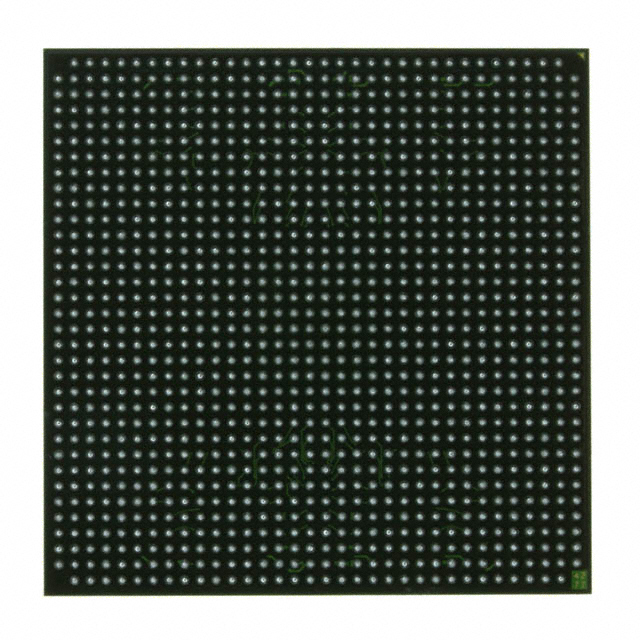
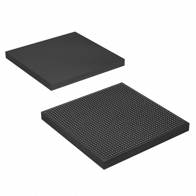
XC2VP50-6FFG1152C
| Part Description |
Virtex®-II Pro Field Programmable Gate Array (FPGA) IC 692 4276224 53136 1152-BBGA, FCBGA |
|---|---|
| Quantity | 673 Available (as of June 14, 2026) |

| Product Category | Field Programmable Gate Array (FPGA) |
|---|---|
| Manufacturer | AMD |
| Manufacturing Status | Obsolete |
| Manufacturer Standard Lead Time | Contact Us |
| Datasheet |
Specifications & Environmental
| Device Package | 1152-FCBGA (35x35) | Grade | Commercial | Operating Temperature | 0°C – 85°C | ||
|---|---|---|---|---|---|---|---|
| Package / Case | 1152-BBGA, FCBGA | Number of I/O | 692 | Voltage | 1.425 V - 1.575 V | ||
| Mounting Method | Surface Mount | RoHS Compliance | ROHS3 Compliant | REACH Compliance | REACH Unaffected | ||
| Moisture Sensitivity Level | 4 (72 Hours) | Number of LABs/CLBs | 5904 | Number of Logic Elements/Cells | 53136 | ||
| Number of Gates | N/A | ECCN | 3A001A7A | HTS Code | 8542.39.0001 | ||
| Qualification | N/A | Total RAM Bits | 4276224 |
Overview of XC2VP50-6FFG1152C – Virtex®-II Pro FPGA (1152‑FCBGA)
The XC2VP50-6FFG1152C is a Virtex®-II Pro Field Programmable Gate Array (FPGA) IC from AMD, supplied in a 1152‑FCBGA (35×35) package. It combines a high logic capacity and on‑chip memory with a large I/O complement and the power/thermal characteristics suitable for commercial‑grade embedded designs.
This device targets applications that require substantial programmable logic, significant embedded RAM, and extensive I/O connectivity while operating within a standard commercial temperature range.
Key Features
- Logic Capacity — 53,136 logic elements to implement complex digital designs and custom processing pipelines.
- Embedded Memory — Approximately 4.28 Mbits of embedded memory (4,276,224 bits) for buffering, FIFOs, and on‑chip data storage.
- I/O — 692 user I/O pins providing broad external interface and high fan‑out connectivity options.
- Power — Core voltage supply range 1.425 V to 1.575 V, supporting stable operation within specified supply limits.
- Package — 1152‑FCBGA (35×35) package case designed for high‑density board routing and thermal performance.
- Operating Range — Commercial grade operation from 0 °C to 85 °C.
- RoHS Compliance — RoHS compliant for environmentally conscious design and supply chain requirements.
- Virtex‑II Pro Family Capabilities — Family‑level features include embedded PowerPC processor block options, RocketIO™ multi‑gigabit transceiver technology, dedicated 18×18 multipliers, digitally controlled impedance I/O, and SelectRAM™ memory hierarchy as documented in the Virtex‑II Pro datasheet.
Typical Applications
- Telecom & Datacom — High I/O count and family support for RocketIO multi‑gigabit transceivers make this device suitable for communications endpoints, interface bridging, and packet processing functions.
- Embedded Processing — Family features that include embedded PowerPC processor blocks enable system integration where on‑chip processing and hardware acceleration are required.
- Signal Processing — Substantial logic element count, dedicated multiplier resources, and embedded RAM support filtering, DSP pipelines, and custom data‑path implementations.
- High‑Density I/O Systems — 692 I/Os and a 1152‑FCBGA package facilitate dense board designs needing many external interfaces or parallel buses.
Unique Advantages
- High programmable capacity: 53,136 logic elements provide the headroom for complex, multi‑function designs.
- Significant on‑chip memory: Approximately 4.28 Mbits of embedded RAM reduces dependence on external memory for many buffering and temporary storage tasks.
- Extensive I/O availability: 692 user I/O pins simplify integration with peripherals, transceivers, and parallel interfaces.
- Commercial temperature suitability: Rated for 0 °C to 85 °C operation for a wide range of standard‑environment applications.
- Package density: 1152‑FCBGA (35×35) supports compact, high‑density PCB layouts while accommodating the device’s pin count.
- Standards‑aware family features: Virtex‑II Pro family documentation describes multi‑gigabit transceivers, embedded processor blocks, and dedicated multiplier and memory resources useful for system designers.
Why Choose XC2VP50-6FFG1152C?
The XC2VP50-6FFG1152C provides a balance of high logic density, substantial embedded memory, and a large number of I/Os in a commercial‑grade Virtex‑II Pro FPGA package. It is suited for engineers who need on‑chip resources to consolidate functions, reduce external components, and implement complex data‑path and control logic within a single device.
With family documentation that includes processor block descriptions, multi‑gigabit transceiver capabilities, and a mature FPGA architecture, this device offers a documented platform for designs that require programmable logic combined with advanced interfacing and embedded memory resources.
Request a quote or contact sales to check availability, lead times, and pricing for the XC2VP50-6FFG1152C. Our team can provide ordering details and support for your procurement needs.


Date Founded: 1969
Headquarters: Santa Clara, California, USA
Employees: 25,000+
Revenue: $22.68 Billion
Certifications and Memberships: ISO9001:2015, RoHS, REACH


