
XC2VP50-6FF1517C
| Part Description |
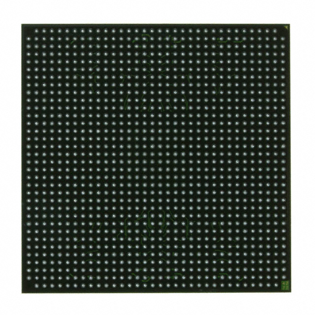
Virtex®-II Pro Field Programmable Gate Array (FPGA) IC 852 4276224 53136 1517-BBGA, FCBGA |
|---|---|
| Quantity | 1,921 Available (as of June 15, 2026) |

| Product Category | Field Programmable Gate Array (FPGA) |
|---|---|
| Manufacturer | AMD |
| Manufacturing Status | Obsolete |
| Manufacturer Standard Lead Time | Contact Us |
| Datasheet |
Specifications & Environmental
| Device Package | 1517-FCBGA (40x40) | Grade | Commercial | Operating Temperature | 0°C – 85°C | ||
|---|---|---|---|---|---|---|---|
| Package / Case | 1517-BBGA, FCBGA | Number of I/O | 852 | Voltage | 1.425 V - 1.575 V | ||
| Mounting Method | Surface Mount | RoHS Compliance | RoHS non-compliant | REACH Compliance | REACH Unaffected | ||
| Moisture Sensitivity Level | 4 (72 Hours) | Number of LABs/CLBs | 5904 | Number of Logic Elements/Cells | 53136 | ||
| Number of Gates | N/A | ECCN | 3A001A7A | HTS Code | 8542.39.0001 | ||
| Qualification | N/A | Total RAM Bits | 4276224 |
Overview of XC2VP50-6FF1517C – Virtex®-II Pro FPGA (1517-FCBGA, Commercial)
The XC2VP50-6FF1517C is a Virtex®-II Pro field-programmable gate array (FPGA) from AMD, provided in a 1517-pin flip-chip BGA (1517-FCBGA, 40×40) package for surface-mount applications. It delivers high-density programmable logic suitable for embedded system integration, communications, and high-performance digital processing.
Key hardware attributes include 53,136 logic elements, approximately 4.276 Mbits of embedded RAM, and up to 852 user I/O pins. The device operates from a 1.425 V to 1.575 V core supply and is specified for commercial temperature operation (0 °C to 85 °C). The Virtex‑II Pro family architecture and supporting documentation provide a platform for integrating processors, multi-gigabit transceivers, and signal-processing blocks where applicable.
Key Features
- High-density logic — 53,136 logic elements for complex digital designs and large-scale integration.
- Embedded memory — Approximately 4.276 Mbits of on-chip RAM to support buffering, frame storage, and intermediate data processing.
- Extensive I/O — Up to 852 user I/O pins to drive dense interface requirements and multiple peripheral buses.
- Package and mounting — 1517-FCBGA (40×40) flip-chip BGA in a surface-mount form factor for compact board-level integration.
- Power supply — Core voltage range of 1.425 V to 1.575 V for compatibility with Virtex‑II Pro power architectures.
- Operating range — Commercial grade temperature specification from 0 °C to 85 °C for standard temperature environments.
- Platform features (family) — Virtex‑II Pro family documentation describes embedded processor block support, RocketIO multi-gigabit transceivers, dedicated multiplier blocks, and comprehensive clock-management resources for system-level design.
- Regulatory — RoHS compliant for lead-free production requirements.
Typical Applications
- Embedded processing and SoC integration — Use the device’s high logic density and the Virtex‑II Pro platform support for integrating processor subsystems and custom accelerators.
- Communications and networking — High I/O count and family-level transceiver capabilities enable aggregation of interfaces and protocol bridging in telecom and datacom systems.
- High-performance signal processing — On-chip RAM and dedicated multiplier resources (documented in the Virtex‑II Pro family materials) support filtering, transforms, and real-time DSP tasks.
- Interface aggregation and protocol conversion — Large number of user I/Os allows consolidation of multiple peripheral and high-speed interfaces on a single device.
Unique Advantages
- High logic capacity: 53,136 logic elements enable implementation of complex state machines, wide datapaths, and large custom logic blocks without partitioning across multiple devices.
- Substantial on-chip memory: Approximately 4.276 Mbits of embedded RAM reduces external memory requirements and accelerates data-intensive functions.
- Large I/O complement: Up to 852 I/Os support dense board-level connectivity and simplify multi-interface designs.
- Compact flip-chip BGA packaging: 1517-FCBGA (40×40) provides a high-pin-count, space-efficient solution suitable for tightly packed PCBs.
- Platform-level design resources: The Virtex‑II Pro family documentation includes architecture descriptions, IP core support, and transceiver/processor functional details to accelerate development.
- Commercial-grade qualification: Specified for 0 °C to 85 °C operation and RoHS compliance for standard commercial applications and production environments.
Why Choose XC2VP50-6FF1517C?
The XC2VP50-6FF1517C is positioned as a high-density Virtex‑II Pro FPGA that combines substantial logic capacity, embedded memory, and a broad I/O complement in a single 1517-FCBGA package. Its specification set makes it suitable for designers who require integrated programmable logic and memory resources to consolidate functions that would otherwise require multiple components.
Designed around the Virtex‑II Pro platform, the device benefits from comprehensive family-level documentation and architecture features that support embedded processing, transceiver integration, and DSP-oriented functions—providing a scalable solution for system architects and procurement teams targeting complex embedded and communications designs.
Request a quote or submit a pricing inquiry to start evaluating the XC2VP50-6FF1517C for your next design.


Date Founded: 1969
Headquarters: Santa Clara, California, USA
Employees: 25,000+
Revenue: $22.68 Billion
Certifications and Memberships: ISO9001:2015, RoHS, REACH


