
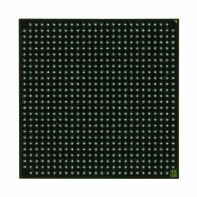
XC2VP7-5FFG672C
| Part Description |
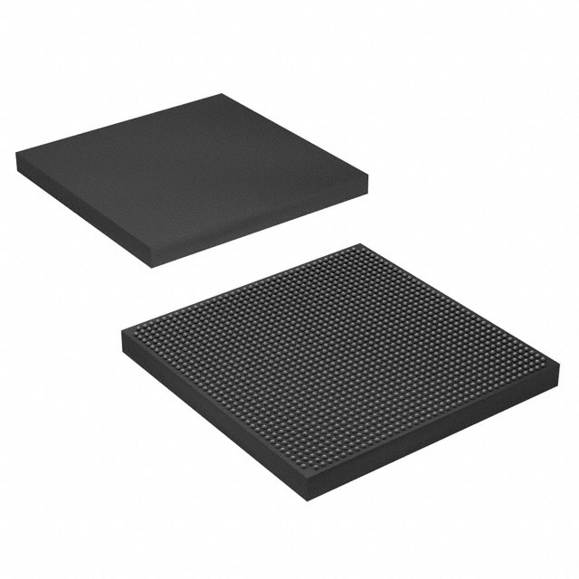
Virtex®-II Pro Field Programmable Gate Array (FPGA) IC 396 811008 11088 672-BBGA, FCBGA |
|---|---|
| Quantity | 193 Available (as of June 15, 2026) |

| Product Category | Field Programmable Gate Array (FPGA) |
|---|---|
| Manufacturer | AMD |
| Manufacturing Status | Obsolete |
| Manufacturer Standard Lead Time | Contact Us |
| Datasheet |
Specifications & Environmental
| Device Package | 672-FCBGA (27x27) | Grade | Commercial | Operating Temperature | 0°C – 85°C | ||
|---|---|---|---|---|---|---|---|
| Package / Case | 672-BBGA, FCBGA | Number of I/O | 396 | Voltage | 1.425 V - 1.575 V | ||
| Mounting Method | Surface Mount | RoHS Compliance | ROHS3 Compliant | REACH Compliance | REACH Unaffected | ||
| Moisture Sensitivity Level | 4 (72 Hours) | Number of LABs/CLBs | 1232 | Number of Logic Elements/Cells | 11088 | ||
| Number of Gates | N/A | ECCN | 3A991D | HTS Code | 8542.39.0001 | ||
| Qualification | N/A | Total RAM Bits | 811008 |
Overview of XC2VP7-5FFG672C – Virtex®-II Pro Field Programmable Gate Array (672‑BBGA FCBGA)
The XC2VP7-5FFG672C is a Virtex®-II Pro family FPGA in a 672‑ball flip‑chip BGA package, optimized for embedded logic and I/O‑dense designs. The device provides a balance of configurable logic, on‑chip memory and high pin‑count I/O for applications that require flexible hardware acceleration and system integration.
As a member of the Virtex‑II Pro family, this device aligns with platform features highlighted in the product specification, including on‑chip memory hierarchy, dedicated multiplier resources and support for processor and multi‑gigabit transceiver integration at the family level.
Key Features
- Logic Resources — 1,232 CLBs delivering 11,088 logic elements for implementing custom logic, state machines and control functions.
- Embedded Memory — Approximately 0.81 Mbits of on‑chip RAM (811,008 total RAM bits) to support buffering, line memory and embedded data storage.
- I/O Capacity — Up to 396 user I/O pins to support parallel interfaces, bus connectivity and board‑level integration.
- Package and Mounting — 672‑BBGA (672‑FCBGA, 27×27 mm) surface‑mount package providing a high‑density footprint for compact board designs.
- Power Supply — Core supply range of 1.425 V to 1.575 V for compatibility with platform power rails.
- Operating Range & Grade — Commercial grade device rated for 0 °C to 85 °C operation and RoHS compliance.
- Family-Level Capabilities — Virtex‑II Pro family features documented in the product specification include embedded PowerPC processor blocks, RocketIO™ multi‑gigabit transceivers, dedicated 18‑bit × 18‑bit multipliers and a SelectRAM™ memory hierarchy for system‑level integration and custom IP support.
Typical Applications
- Telecommunications & Datacom — Use where dense I/O and family‑level multi‑gigabit transceiver support enable serial interface implementations and board‑level protocol processing.
- Embedded Processing — Ideal for designs that leverage on‑chip logic and family‑level embedded processor blocks for control and protocol handling.
- Signal Processing & Acceleration — Deploy for arithmetic‑intensive functions using the device’s dedicated multiplier resources and embedded RAM for intermediate data storage.
- High‑Pin‑Count System Integration — Suited to applications that require many parallel interfaces or extensive peripheral connectivity enabled by 396 I/O pins.
Unique Advantages
- Balanced Logic and Memory — Combines 11,088 logic elements with approximately 0.81 Mbits of embedded RAM to implement control logic and local data storage without external memory for many use cases.
- High I/O Density — 396 I/O pins in a 672‑ball FCBGA package enable complex board interconnects and multiple parallel interfaces in a compact footprint.
- Platform Ecosystem — Part of the Virtex‑II Pro family, which provides documented support for embedded processors, multi‑gigabit transceivers and IP cores according to the product specification.
- Industry‑Standard Package — 27×27 mm 672‑FCBGA supports surface‑mount production and high‑density PCB layouts.
- Regulatory & Environmental — RoHS‑compliant construction aligns with common manufacturing and environmental requirements.
Why Choose XC2VP7-5FFG672C?
The XC2VP7-5FFG672C delivers a robust combination of configurable logic, embedded memory and high I/O count in a 672‑ball FCBGA package, making it suitable for engineers who need on‑board acceleration, extensive peripheral connectivity and platform-level integration. Its device specifications—11,088 logic elements, approximately 0.81 Mbits of RAM and 396 I/O—allow designers to consolidate functions and simplify system architecture.
As a Virtex‑II Pro family device, it benefits from the platform’s documented capabilities for embedded processing, multi‑gigabit serial interfaces and dedicated arithmetic resources, providing a practical choice for mid‑to‑high complexity FPGA designs where modular IP and hardware flexibility are important.
Request a quote or submit an inquiry to receive pricing and availability information for the XC2VP7-5FFG672C.


Date Founded: 1969
Headquarters: Santa Clara, California, USA
Employees: 25,000+
Revenue: $22.68 Billion
Certifications and Memberships: ISO9001:2015, RoHS, REACH


