
XC2VP7-6FF896I
| Part Description |
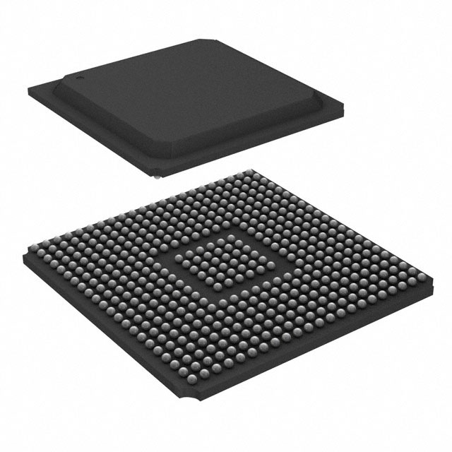
Virtex®-II Pro Field Programmable Gate Array (FPGA) IC 396 811008 11088 896-BBGA, FCBGA |
|---|---|
| Quantity | 120 Available (as of June 14, 2026) |

| Product Category | Field Programmable Gate Array (FPGA) |
|---|---|
| Manufacturer | AMD |
| Manufacturing Status | Obsolete |
| Manufacturer Standard Lead Time | Contact Us |
| Datasheet |
Specifications & Environmental
| Device Package | 896-FCBGA (31x31) | Grade | Industrial | Operating Temperature | -40°C – 100°C | ||
|---|---|---|---|---|---|---|---|
| Package / Case | 896-BBGA, FCBGA | Number of I/O | 396 | Voltage | 1.425 V - 1.575 V | ||
| Mounting Method | Surface Mount | RoHS Compliance | RoHS non-compliant | REACH Compliance | REACH Unaffected | ||
| Moisture Sensitivity Level | 4 (72 Hours) | Number of LABs/CLBs | 1232 | Number of Logic Elements/Cells | 11088 | ||
| Number of Gates | N/A | ECCN | 3A991D | HTS Code | 8542.39.0001 | ||
| Qualification | N/A | Total RAM Bits | 811008 |
Overview of XC2VP7-6FF896I – Virtex®-II Pro Field Programmable Gate Array, 396 I/O, 896-FCBGA
The XC2VP7-6FF896I is an industrial-grade Virtex®-II Pro platform FPGA from AMD provided in a 896‑ball FCBGA package. It combines a configurable logic fabric with on-chip memory and a high-density I/O footprint, making it suitable for embedded processing and high-performance digital designs that require robust temperature and voltage operation.
Key Features
- Logic Capacity: 11,088 logic elements (logic cells) to implement complex digital functions and custom hardware accelerators.
- Embedded Memory: Approximately 0.81 Mbits of on-chip RAM for data buffering, FIFOs, and local storage.
- I/O Density: 396 user I/O pins to support wide external interfaces and parallel buses.
- Package: 896‑BBGA / 896‑FCBGA in a 31 × 31 mm footprint for high pin-count, surface-mount PCB assembly.
- Power Supply: Core voltage range 1.425 V to 1.575 V to match typical FPGA power rails.
- Temperature Range: Industrial operating range from -40 °C to 100 °C for deployment in demanding environments.
- Platform Capabilities (family-level): Virtex‑II Pro family features include embedded PowerPC™ processor blocks, RocketIO™ multi‑gigabit transceivers, SelectRAM™+ memory hierarchy, 18‑bit × 18‑bit multiplier blocks, digitally controlled impedance I/O (DCI), on‑chip differential termination, digital clock manager (DCM), and SelectI/O™‑Ultra technology as documented in the Virtex‑II Pro product specification.
- Mounting & Compliance: Surface-mount package with RoHS compliance for modern assembly requirements.
Typical Applications
- Embedded processing systems: Implement custom processor interfaces, hardware accelerators, or offload tasks using the Virtex‑II Pro platform features.
- High-speed communications: Use the family’s RocketIO transceiver and high I/O count for serial links and board-level protocol bridging.
- Industrial control and automation: Leverage the industrial temperature rating and dense I/O for motor control, sensor aggregation, and real‑time logic.
- Data buffering and interfacing: On-chip RAM and plentiful I/O enable data staging, protocol conversion, and wide parallel bus implementations.
Unique Advantages
- High functional density: 11,088 logic elements combined with approximately 0.81 Mbits of embedded RAM reduce external component needs and simplify system architecture.
- Large I/O surface: 396 I/O pins in a compact 896‑FCBGA package enable integration of multiple peripherals and wide data buses without sacrificing board area efficiency.
- Industrial robustness: Rated for -40 °C to 100 °C operation, supporting deployments in harsh or temperature‑variable environments.
- Platform-level processing and transceivers: Family-documented support for embedded PowerPC cores and RocketIO multi‑gigabit transceivers enables mixed-signal system designs and high-throughput interfaces where required.
- Documented architecture and IP support: Comprehensive product specification coverage (architecture, I/O, clocking, memory, and transceiver function) aids design planning and integration.
- Compliance-ready assembly: Surface-mount 896‑FCBGA package and RoHS compliance align with modern PCB manufacturing processes.
Why Choose XC2VP7-6FF896I?
The XC2VP7-6FF896I positions itself as a versatile Virtex‑II Pro platform FPGA option for designers needing a balance of logic capacity, embedded memory, and a high I/O count in an industrial‑rated package. Its documented family features—such as embedded processor blocks, multi‑gigabit transceiver capability, dedicated multiplier blocks, and advanced I/O management—support engineered solutions that combine programmable logic with embedded processing and high-speed interfaces.
This device is appropriate for engineering teams building industrial controls, communications interfaces, or embedded systems that require scalable logic resources, on-chip memory, and a robust operating range, while benefiting from the detailed product specification and IP core references available for the Virtex‑II Pro family.
Request a quote or submit an inquiry to receive pricing and availability information for the XC2VP7-6FF896I. Our team will respond with lead-time and ordering options tailored to your project needs.


Date Founded: 1969
Headquarters: Santa Clara, California, USA
Employees: 25,000+
Revenue: $22.68 Billion
Certifications and Memberships: ISO9001:2015, RoHS, REACH


