
XC2VP7-6FFG896C
| Part Description |
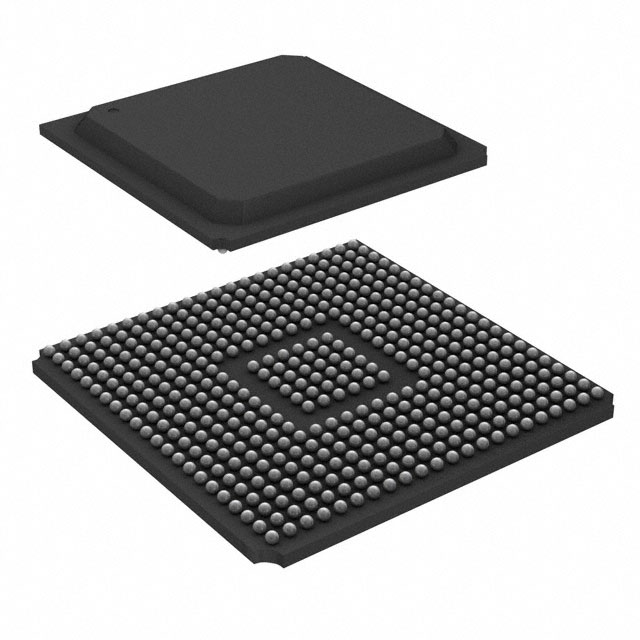
Virtex®-II Pro Field Programmable Gate Array (FPGA) IC 396 811008 11088 896-BBGA, FCBGA |
|---|---|
| Quantity | 874 Available (as of October 7, 2026) |

| Product Category | Field Programmable Gate Array (FPGA) |
|---|---|
| Manufacturer | AMD |
| Manufacturing Status | Obsolete |
| Manufacturer Standard Lead Time | Contact Us |
| Datasheet |
Specifications & Environmental
| Device Package | 896-FCBGA (31x31) | Grade | Commercial | Operating Temperature | 0°C – 85°C | ||
|---|---|---|---|---|---|---|---|
| Package / Case | 896-BBGA, FCBGA | Number of I/O | 396 | Voltage | 1.425 V - 1.575 V | ||
| Mounting Method | Surface Mount | RoHS Compliance | ROHS3 Compliant | REACH Compliance | REACH Unaffected | ||
| Moisture Sensitivity Level | 4 (72 Hours) | Number of LABs/CLBs | 1232 | Number of Logic Elements/Cells | 11088 | ||
| Number of Gates | N/A | ECCN | 3A991D | HTS Code | 8542.39.0001 | ||
| Qualification | N/A | Total RAM Bits | 811008 |
Overview of XC2VP7-6FFG896C – Virtex®-II Pro Field Programmable Gate Array (FPGA), 896‑FCBGA (31×31)
The XC2VP7-6FFG896C is a commercial-grade Virtex®-II Pro FPGA in a 896‑FCBGA (31×31) surface-mount package from AMD. It combines a flexible FPGA fabric with the platform features of the Virtex‑II Pro family to address embedded processing and high‑performance I/O use cases.
This device provides a balance of logic capacity, embedded memory and a high pin count for system integration in applications requiring on‑chip processing, custom logic and high-speed interfaces within a commercial temperature range.
Key Features
- Logic Capacity – Approximately 11,088 logic elements, supported by 1,232 configurable logic blocks (CLBs) for implementing custom digital functions and control logic.
- Embedded Memory – Approximately 0.81 Mbits of embedded RAM (811,008 total RAM bits) to support FIFOs, buffering and local data storage.
- I/O Resources – Up to 396 user I/O pins to interface with external peripherals, sensors and high‑speed devices.
- Power and Supply – Core supply voltage range of 1.425 V to 1.575 V, enabling designs that require tightly defined core-voltage operation.
- Package and Mounting – 896‑BBGA / 896‑FCBGA package (31×31 mm), surface-mount for compact board-level integration.
- Operating Range – Commercial operating temperature from 0 °C to 85 °C for standard commercial applications.
- RoHS Compliant – Device meets RoHS requirements for lead‑free manufacturing and environmental compliance.
- Virtex‑II Pro Platform Features – Family-level capabilities include embedded processor blocks (PowerPC™ 405 cores), RocketIO™/RocketIO X multi‑gigabit transceivers, dedicated 18‑bit × 18‑bit multiplier blocks, on‑chip SelectRAM™ memory hierarchy and digital clock management resources (as documented in the Virtex‑II Pro family datasheet).
Typical Applications
- High‑speed Communications – Implement line interfaces, protocol bridging and data-path functions leveraging the family’s RocketIO transceiver support and high I/O count.
- Embedded Processing Systems – Integrate control and data‑plane tasks using the platform’s embedded processor block options together with FPGA fabric for custom acceleration.
- Digital Signal Processing – Use on‑chip RAM and dedicated multiplier blocks for real‑time DSP algorithms, filtering and streaming data processing.
- Custom System Integration – Consolidate glue logic, sensor interfaces and peripheral control in a single FPGA device to reduce PCB complexity and bill of materials.
Unique Advantages
- Balanced Logic and Memory – Approximately 11,088 logic elements paired with ~0.81 Mbits of embedded memory enable mid‑range FPGA designs with local buffering and state storage.
- High Pin Count for I/O‑Rich Designs – 396 I/Os accommodate wide buses, parallel interfaces and multiple peripheral connections without external expander ICs.
- Platform-Level Integration – Virtex‑II Pro family features such as embedded processor blocks and multi‑gigabit transceivers simplify system architectures that require both programmable logic and embedded processing.
- Surface‑Mount, High‑Density Package – The 896‑FCBGA (31×31) package supports compact, high‑density board layouts for space‑constrained products.
- Commercial Temperature Qualification – Rated for 0 °C to 85 °C operation for mainstream electronics and commercial applications.
- Regulatory Compliance – RoHS‑compliant supply reduces regulatory risk in lead‑free manufacturing flows.
Why Choose XC2VP7-6FFG896C?
The XC2VP7-6FFG896C offers a practical combination of logic resources, embedded memory and extensive I/O in a compact 896‑FCBGA package for commercial applications. Its placement within the Virtex‑II Pro family provides access to platform features—such as embedded processor blocks and high‑speed transceiver support—enabling integrated designs that merge programmable logic with embedded processing and high‑bandwidth interfaces.
This device is well suited to engineers and teams building mid‑range FPGA systems that require on‑chip memory, significant I/O connectivity and a commercially rated temperature range, while benefiting from the documented Virtex‑II Pro family architecture and resources.
Request a quote or submit an inquiry for pricing and availability of XC2VP7-6FFG896C to evaluate it for your next design.























Date Founded: 1969
Headquarters: Santa Clara, California, USA
Employees: 25,000+
Revenue: $22.68 Billion
Certifications and Memberships: ISO9001:2015, RoHS, REACH











