
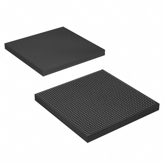
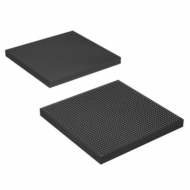
XC2VP70-6FFG1517C
| Part Description |
Virtex®-II Pro Field Programmable Gate Array (FPGA) IC 964 6045696 74448 1517-BBGA, FCBGA |
|---|---|
| Quantity | 198 Available (as of October 8, 2026) |

| Product Category | Field Programmable Gate Array (FPGA) |
|---|---|
| Manufacturer | AMD |
| Manufacturing Status | Obsolete |
| Manufacturer Standard Lead Time | Contact Us |
| Datasheet |
Specifications & Environmental
| Device Package | 1517-FCBGA (40x40) | Grade | Commercial | Operating Temperature | 0°C – 85°C | ||
|---|---|---|---|---|---|---|---|
| Package / Case | 1517-BBGA, FCBGA | Number of I/O | 964 | Voltage | 1.425 V - 1.575 V | ||
| Mounting Method | Surface Mount | RoHS Compliance | ROHS3 Compliant | REACH Compliance | REACH Unaffected | ||
| Moisture Sensitivity Level | 4 (72 Hours) | Number of LABs/CLBs | 8272 | Number of Logic Elements/Cells | 74448 | ||
| Number of Gates | N/A | ECCN | 3A001A7A | HTS Code | 8542.39.0001 | ||
| Qualification | N/A | Total RAM Bits | 6045696 |
Overview of XC2VP70-6FFG1517C – Virtex®-II Pro Field Programmable Gate Array (FPGA) IC
The XC2VP70-6FFG1517C is a Virtex®-II Pro family FPGA from AMD supplied in a 1517-FCBGA (40×40) package. It combines high logic density, embedded memory and rich I/O to address complex embedded processing, high-density logic implementation, and multi-gigabit interface applications.
Built on the Virtex-II Pro platform architecture, this device integrates configurable logic, dedicated DSP multipliers, on-chip memory, and family support for embedded processor blocks and multi‑gigabit transceivers, enabling system-level integration for communication and embedded systems designs.
Key Features
- Logic Capacity Provides 8,272 CLBs and 74,448 logic elements for implementing large-scale FPGA designs and complex logic functions.
- Embedded Memory Approximately 6.05 Mbits of on-chip RAM (6,045,696 bits) to support buffering, FIFOs and block memory requirements within the FPGA fabric.
- DSP Resources Includes dedicated 18‑bit × 18‑bit multiplier resources as part of the Virtex‑II Pro architecture for efficient signal processing and multiply‑accumulate tasks.
- I/O Density Up to 964 I/O pins provide extensive connectivity for high‑pin‑count systems and board-level integration.
- Embedded Processors & Transceivers Family-level support includes embedded processor blocks (up to two IBM PowerPC™ cores) and up to twenty RocketIO or RocketIO X multi‑gigabit transceivers for high‑speed serial links and embedded processing platforms.
- Clocking and I/O Technology Features high-performance clock management and SelectI/O™-Ultra family technologies (documented in the device data) to enable flexible clocking and I/O configurations.
- Package & Mounting Supplied in a 1517‑BBGA (FCBGA) package, 40×40 format, for surface-mount PCB assembly in compact, high-density designs.
- Power and Temperature Core supply range 1.425 V to 1.575 V; commercial operating temperature range 0 °C to 85 °C.
- Compliance RoHS compliant for regulatory and manufacturing requirements.
Typical Applications
- Embedded Processing Systems Leverage on‑chip processor block support and abundant logic/memory to implement system controllers and application-specific processing subsystems.
- Telecom & Datacom Use the family’s RocketIO multi‑gigabit transceiver support and high I/O count for serial links, backplane interfaces and communication protocol implementations.
- Signal Processing Dedicated 18×18 multipliers and substantial on‑chip RAM enable filtering, transform engines and other DSP workflows within the FPGA fabric.
- High‑Density Logic Integration High logic element count and wide I/O allow consolidation of multiple functions into a single FPGA for complex control, switching or protocol aggregation tasks.
Unique Advantages
- High logic and memory integration: Combines 74,448 logic elements with approximately 6.05 Mbits of embedded RAM to reduce external memory and logic partitioning.
- Extensive I/O and package density: 964 I/Os in a 1517‑FCBGA package support high‑pin‑count applications while keeping a compact board footprint.
- Embedded processing capability: Family support for up to two PowerPC processor blocks simplifies implementation of-software-plus-hardware systems on a single device.
- High-speed serial support: Family-level RocketIO transceivers provide options for multi‑gigabit connectivity suitable for telecom and datacom interfaces.
- Design ecosystem documentation: Comprehensive device documentation and IP/core reference support are available for integration and development.
- Regulatory readiness: RoHS compliance supports current manufacturing and environmental requirements.
Why Choose XC2VP70-6FFG1517C?
The XC2VP70-6FFG1517C positions itself as a high-capacity Virtex‑II Pro FPGA option when designers require large logic arrays, significant on‑chip memory, and broad I/O in a 1517‑FCBGA package. Its combination of logic elements, embedded RAM and family‑level support for embedded processors and multi‑gigabit transceivers makes it suitable for integrated communication, signal processing and embedded compute applications.
For teams targeting robust, documented FPGA solutions with family-level IP and reference support, the XC2VP70-6FFG1517C offers a balanced mix of compute fabric, memory and connectivity in a commercial-grade device.
Request a quote or submit an inquiry to check availability, pricing and lead time for the XC2VP70-6FFG1517C.























Date Founded: 1969
Headquarters: Santa Clara, California, USA
Employees: 25,000+
Revenue: $22.68 Billion
Certifications and Memberships: ISO9001:2015, RoHS, REACH











