
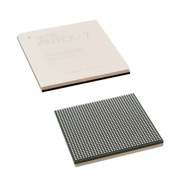
XC7K410T-L2FFG900E
| Part Description |
Kintex®-7 Field Programmable Gate Array (FPGA) IC 500 29306880 406720 900-BBGA, FCBGA |
|---|---|
| Quantity | 407 Available (as of June 18, 2026) |
| Product Category | Field Programmable Gate Array (FPGA) |
|---|---|
| Manufacturer | AMD |
| Manufacturing Status | Active |
| Manufacturer Standard Lead Time | 16 Weeks |
| Datasheet |
Specifications & Environmental
| Device Package | 900-FCBGA (31x31) | Grade | Extended | Operating Temperature | 0°C – 100°C | ||
|---|---|---|---|---|---|---|---|
| Package / Case | 900-BBGA, FCBGA | Number of I/O | 500 | Voltage | 970 mV - 1.03 V | ||
| Mounting Method | Surface Mount | RoHS Compliance | ROHS3 Compliant | REACH Compliance | REACH Unaffected | ||
| Moisture Sensitivity Level | 4 (72 Hours) | Number of LABs/CLBs | 31775 | Number of Logic Elements/Cells | 406720 | ||
| Number of Gates | N/A | ECCN | 3A991D | HTS Code | 8542.39.0001 | ||
| Qualification | N/A | Total RAM Bits | 29306880 |
Overview of XC7K410T-L2FFG900E – Kintex®-7 FPGA (AMD), 900‑FCBGA (31×31), Extended Grade
The XC7K410T-L2FFG900E is a Kintex®-7 Field Programmable Gate Array (FPGA) IC from AMD packaged in a 900‑ball FCBGA (31×31) footprint. It delivers high logic capacity, substantial on‑chip memory, and a large I/O complement for demanding programmable-logic designs.
With 406,720 logic elements, approximately 29.3 Mbits of embedded memory and 500 I/O, this device supports designs that require dense logic integration, significant local RAM resources and extensive external connectivity while operating in an extended temperature range.
Key Features
- High Logic Density 406,720 logic elements to implement complex digital functions and parallel processing structures.
- Embedded Memory Approximately 29.3 Mbits of on‑chip RAM to support buffering, lookup tables and local data storage without external memory.
- Large I/O Count 500 user I/O pins to accommodate multi‑channel interfaces and high‑pin‑count system connections.
- Package and Mounting 900‑ball FCBGA package (900‑FCBGA, 31×31) optimized for surface‑mount board assembly and dense PCB layouts.
- Power Supply Range Core supply specified from 970 mV to 1.03 V to match system power rails and regulatory requirements for core voltage.
- Operating Temperature Rated for 0 °C to 100 °C operation consistent with extended‑grade deployment scenarios.
- Environmental Compliance RoHS compliant for reduced hazardous substance content.
Typical Applications
- Custom Digital Processing Implement complex, high‑density logic and custom datapaths using the device’s large logic element count.
- Memory‑Intensive Functions Use the approximately 29.3 Mbits of embedded RAM for buffering, packet queues, and local storage in data‑centric designs.
- Multi‑I/O Systems Support applications requiring many parallel interfaces or channelized I/O with the 500 available I/O pins.
Unique Advantages
- High integration density: 406,720 logic elements allow consolidation of multiple functions into a single FPGA, reducing board-level complexity.
- Substantial embedded memory: Approximately 29.3 Mbits of on‑chip RAM reduces dependence on external memory and improves data locality.
- Rich I/O capability: 500 I/O pins provide flexibility for interfacing to numerous peripherals and high‑channel systems.
- Compact, surface‑mount FCBGA package: 900‑FCBGA (31×31) supports high‑density PCB layouts and standardized assembly processes.
- Extended grade operation: Specified for 0 °C to 100 °C, enabling deployment in environments that require extended temperature tolerance.
- Regulatory compliance: RoHS compliance supports environmental and manufacturing requirements.
Why Choose XC7K410T-L2FFG900E?
The XC7K410T-L2FFG900E positions itself for designs that demand significant programmable logic capacity, generous on‑chip RAM and broad I/O connectivity in a compact FCBGA package. Its combination of 406,720 logic elements, approximately 29.3 Mbits of embedded memory and 500 I/O make it suitable for consolidating complex digital functions and reducing external component count.
Specified for core voltages from 970 mV to 1.03 V and rated for 0 °C to 100 °C operation, this extended‑grade Kintex®‑7 FPGA provides a balance of integration, configurability and environmental robustness for long‑life, high‑density designs backed by AMD’s Kintex‑7 family documentation and support.
Request a quote or submit an inquiry to obtain pricing, lead time and availability for the XC7K410T-L2FFG900E. Our team can provide technical and procurement assistance to support your design and sourcing needs.


Date Founded: 1969
Headquarters: Santa Clara, California, USA
Employees: 25,000+
Revenue: $22.68 Billion
Certifications and Memberships: ISO9001:2015, RoHS, REACH


