
XC7VX1140T-L2FLG1928E
| Part Description |
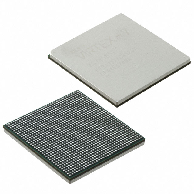
Virtex®-7 XT Field Programmable Gate Array (FPGA) IC 480 69304320 1139200 1924-BBGA, FCBGA |
|---|---|
| Quantity | 714 Available (as of June 15, 2026) |

| Product Category | Field Programmable Gate Array (FPGA) |
|---|---|
| Manufacturer | AMD |
| Manufacturing Status | Active |
| Manufacturer Standard Lead Time | 20 Weeks |
| Datasheet |
Specifications & Environmental
| Device Package | 1928-FCBGA (45x45) | Grade | Extended | Operating Temperature | 0°C – 100°C | ||
|---|---|---|---|---|---|---|---|
| Package / Case | 1924-BBGA, FCBGA | Number of I/O | 480 | Voltage | 970 mV - 1.03 V | ||
| Mounting Method | Surface Mount | RoHS Compliance | RoHS non-compliant | REACH Compliance | REACH Unaffected | ||
| Moisture Sensitivity Level | 4 (72 Hours) | Number of LABs/CLBs | 89000 | Number of Logic Elements/Cells | 1139200 | ||
| Number of Gates | N/A | ECCN | 3A001A7B | HTS Code | 8542.39.0001 | ||
| Qualification | N/A | Total RAM Bits | 69304320 |
Overview of XC7VX1140T-L2FLG1928E – Virtex‑7 XT FPGA, 1928‑FCBGA
The XC7VX1140T-L2FLG1928E is a Virtex®-7 XT field programmable gate array (FPGA) IC offered in a high‑pin FCBGA package. It delivers very large logic capacity, substantial on‑chip memory, and a high I/O count for complex digital designs.
Designed for applications that require extensive programmable logic, embedded memory, and numerous I/O connections, this extended‑grade device provides a compact surface‑mount solution with a 0 °C to 100 °C operating range and a core supply range of 0.970 V to 1.03 V.
Key Features
- Logic Capacity Approximately 89,000 CLBs and 1,139,200 logic elements provide the programmable resources needed for large finite state machines, custom datapaths, and parallel processing implementations.
- Embedded Memory Approximately 69 Mbits of on‑chip RAM offer substantial storage for buffering, lookup tables, and algorithm state without external memory.
- I/O Resources 480 user I/O pins enable dense external connectivity for multi‑lane interfaces, sensor arrays, or complex peripheral sets.
- Power and Core Supply Core voltage supply specified from 0.970 V to 1.03 V to match system power delivery and voltage rail planning.
- Package and Mounting Surface‑mount FCBGA package: Supplier device package 1928‑FCBGA (45×45) with package case 1924‑BBGA, providing a high‑pin count footprint for compact board designs.
- Extended Temperature Grade Rated for operation from 0 °C to 100 °C, suitable for applications requiring extended commercial temperature performance.
- Environmental Compliance RoHS compliant.
Typical Applications
- High‑density logic implementations Large combinational and sequential designs that require extensive logic elements and CLBs can be mapped directly onto the device’s capacity.
- Memory‑intensive functions Embedded RAM (~69 Mbits) supports buffering, lookup tables, and data staging for algorithms that need significant on‑chip storage.
- I/O‑rich systems Applications requiring hundreds of external connections can leverage the 480 I/O pins for multi‑lane interfaces, parallel sensors, or extensive peripheral control.
Unique Advantages
- Very high logic density: Over one million logic elements enable consolidation of complex subsystems into a single FPGA, reducing PCB count and interconnect complexity.
- Substantial on‑chip memory: Approximately 69 Mbits of embedded RAM minimizes dependence on external memory and lowers system latency for memory‑bound tasks.
- Large I/O complement: 480 I/O pins provide flexibility for integrating multiple external devices and high‑bandwidth interfaces without multiplexing compromises.
- Compact high‑pin package: 1928‑FCBGA (45×45) package supports a high number of signals in a compact footprint for dense board layouts.
- Extended operating range: 0 °C to 100 °C qualification fits applications needing extended commercial temperature performance.
- RoHS compliant: Meets environmental compliance requirements for assembly and procurement.
Why Choose XC7VX1140T-L2FLG1928E?
The XC7VX1140T-L2FLG1928E positions itself as a high‑capacity Virtex‑7 XT FPGA tailored for designers who need a large pool of programmable logic, substantial embedded memory, and extensive I/O in a single surface‑mount package. Its combination of roughly 1,139,200 logic elements, approximately 69 Mbits of RAM, and 480 I/Os enables integration of complex digital subsystems while simplifying board‑level architecture.
This extended‑grade device is suited to designers seeking scalability and integration for demanding digital tasks, where consolidating functions into a single FPGA reduces BOM complexity and streamlines system design. Manufacturer documentation is available for detailed series specifications and design guidance.
Request a quote or submit a product inquiry to receive pricing and availability for the XC7VX1140T-L2FLG1928E. Our team can assist with order placement and technical procurement details.


Date Founded: 1969
Headquarters: Santa Clara, California, USA
Employees: 25,000+
Revenue: $22.68 Billion
Certifications and Memberships: ISO9001:2015, RoHS, REACH


