
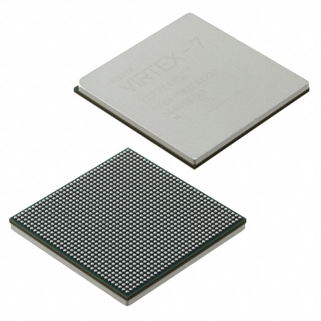
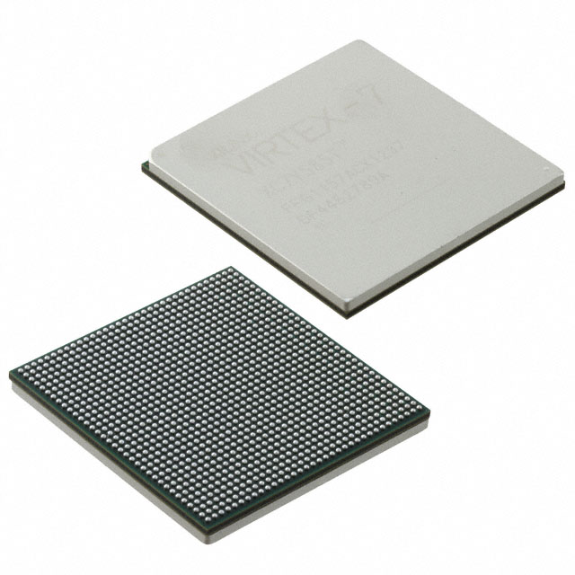
XC7VX550T-2FFG1158C
| Part Description |
Virtex®-7 XT Field Programmable Gate Array (FPGA) IC 350 43499520 554240 1156-BBGA, FCBGA |
|---|---|
| Quantity | 198 Available (as of June 15, 2026) |
| Product Category | Field Programmable Gate Array (FPGA) |
|---|---|
| Manufacturer | AMD |
| Manufacturing Status | Active |
| Manufacturer Standard Lead Time | 16 Weeks |
| Datasheet |
Specifications & Environmental
| Device Package | 1158-FCBGA (35x35) | Grade | Commercial | Operating Temperature | 0°C – 85°C | ||
|---|---|---|---|---|---|---|---|
| Package / Case | 1156-BBGA, FCBGA | Number of I/O | 350 | Voltage | 970 mV - 1.03 V | ||
| Mounting Method | Surface Mount | RoHS Compliance | ROHS3 Compliant | REACH Compliance | REACH Unaffected | ||
| Moisture Sensitivity Level | 4 (72 Hours) | Number of LABs/CLBs | 43300 | Number of Logic Elements/Cells | 554240 | ||
| Number of Gates | N/A | ECCN | 3A001A7B | HTS Code | 8542.39.0001 | ||
| Qualification | N/A | Total RAM Bits | 43499520 |
Overview of XC7VX550T-2FFG1158C – Virtex®-7 XT Field Programmable Gate Array (FPGA), 1156-BBGA FCBGA
The XC7VX550T-2FFG1158C is a Virtex®-7 XT Field Programmable Gate Array (FPGA) from AMD, delivered in an FCBGA surface-mount package. It combines a large logic fabric with substantial on-chip memory and a high I/O count to address demanding programmable-logic designs.
Key device attributes include approximately 554,240 logic elements, roughly 43.5 Mbits of embedded memory, 350 I/O pins, a narrow core supply range (0.97 V to 1.03 V), and commercial-grade operation from 0 °C to 85 °C.
Key Features
- Core Logic – Approximately 554,240 logic elements (cells) provide extensive capacity for large-scale logic implementation and complex digital designs.
- Configurable Logic Blocks (CLBs) – About 43,300 CLBs available for flexible partitioning of logic and routing resources.
- Embedded Memory – Approximately 43.5 Mbits of on-chip RAM to support buffering, lookup tables, and local data storage without relying solely on external memory.
- I/O Capability – 350 user I/O pins to support multiple interfaces and high pin-count connectivity requirements.
- Power – Core voltage supply range of 0.97 V to 1.03 V to match tight power delivery requirements for the device.
- Package & Mounting – Surface-mount FCBGA package; package case listed as 1156-BBGA, FCBGA with supplier device package 1158-FCBGA (35×35), suitable for compact, high-density board layouts.
- Operating Range & Grade – Commercial-grade device with an operating temperature range of 0 °C to 85 °C.
- Environmental Compliance – RoHS compliant.
Typical Applications
- High-density programmable logic systems – Use the large logic element count and CLB resources for complex custom logic implementations and hardware acceleration.
- Data buffering and local memory tasks – Approximately 43.5 Mbits of embedded RAM supports on-chip storage for buffering and intermediate data processing.
- I/O-intensive interface aggregation – 350 I/O pins enable consolidation of multiple interfaces and high connection density on a single FPGA.
- Platform prototyping and system integration – Commercial-grade operation and surface-mount FCBGA packaging make the device suitable for development platforms and integrated system designs.
Unique Advantages
- Large on-chip logic capacity: With roughly 554,240 logic elements, the device supports complex designs without immediate need for partitioning across multiple FPGAs.
- Significant embedded memory: Approximately 43.5 Mbits of RAM reduces dependence on external memory components for many buffering and storage tasks.
- High I/O count: 350 I/O pins allow integration of multiple peripherals and interfaces directly to the FPGA, simplifying board-level interconnect.
- Compact, high-density package: FCBGA packaging and a 35×35 supplier footprint support dense PCB layouts and space-constrained designs.
- Narrow core supply range: A defined voltage window (0.97 V–1.03 V) aids in predictable power delivery and planning for the core supply rail.
- RoHS compliant commercial device: Meets RoHS requirements for environmentally conscious product designs within standard commercial temperature ranges.
Why Choose XC7VX550T-2FFG1158C?
The XC7VX550T-2FFG1158C positions itself as a high-capacity Virtex®-7 XT FPGA option for designs that require extensive logic resources, sizeable on-chip memory, and a large number of I/O connections. Its combination of approximately 554,240 logic elements, around 43.5 Mbits of embedded RAM, and 350 I/Os provides a strong foundation for consolidating functions that would otherwise require multiple components.
Targeted at commercial-grade applications operating from 0 °C to 85 °C, the device offers a compact FCBGA footprint and RoHS compliance for streamlined integration. Choose this FPGA when your design priorities include high integration density, substantial local memory, and broad I/O capability backed by the Virtex-7 product family.
Request a quote or submit a pricing inquiry today to check availability and get further purchasing information for XC7VX550T-2FFG1158C.


Date Founded: 1969
Headquarters: Santa Clara, California, USA
Employees: 25,000+
Revenue: $22.68 Billion
Certifications and Memberships: ISO9001:2015, RoHS, REACH


