
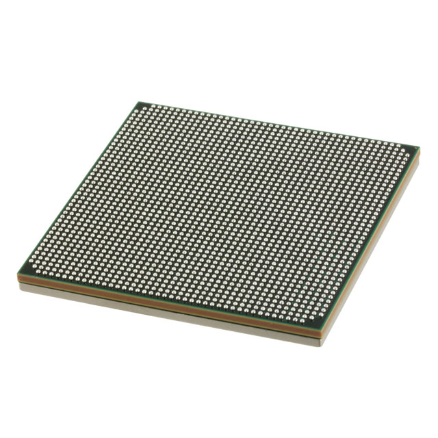
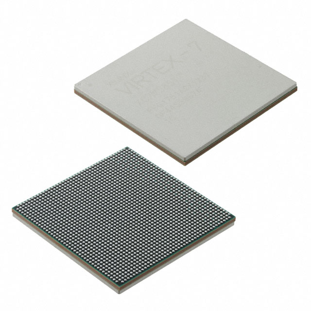
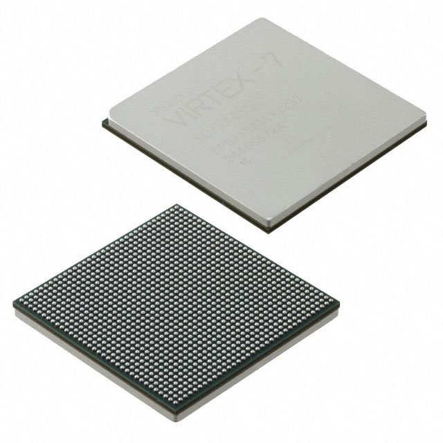
XC7VX690T-L2FFG1926E
| Part Description |
Virtex®-7 XT Field Programmable Gate Array (FPGA) IC 720 54190080 693120 1924-BBGA, FCBGA |
|---|---|
| Quantity | 993 Available (as of June 18, 2026) |
| Product Category | Field Programmable Gate Array (FPGA) |
|---|---|
| Manufacturer | AMD |
| Manufacturing Status | Active |
| Manufacturer Standard Lead Time | 16 Weeks |
| Datasheet |
Specifications & Environmental
| Device Package | 1926-FCBGA (45x45) | Grade | Extended | Operating Temperature | 0°C – 100°C | ||
|---|---|---|---|---|---|---|---|
| Package / Case | 1924-BBGA, FCBGA | Number of I/O | 720 | Voltage | 970 mV - 1.03 V | ||
| Mounting Method | Surface Mount | RoHS Compliance | ROHS3 Compliant | REACH Compliance | REACH Unaffected | ||
| Moisture Sensitivity Level | 4 (72 Hours) | Number of LABs/CLBs | 54150 | Number of Logic Elements/Cells | 693120 | ||
| Number of Gates | N/A | ECCN | 3A001A7A | HTS Code | 8542.39.0001 | ||
| Qualification | N/A | Total RAM Bits | 54190080 |
Overview of XC7VX690T-L2FFG1926E – Virtex®-7 XT Field Programmable Gate Array (FPGA)
The XC7VX690T-L2FFG1926E is a Virtex®-7 XT field programmable gate array offering a large logic and memory footprint for complex, programmable digital designs. It combines 693,120 logic elements (cells), approximately 54 Mbits of on-chip RAM, and up to 720 user I/Os in a high-pin-count FCBGA package.
Targeted at applications that require substantial programmable logic, high I/O density, and on-chip memory, this extended-grade, surface-mount FPGA provides a compact integration point for advanced communications, signal processing, and custom hardware acceleration designs.
Key Features
- Logic Capacity — 693,120 logic elements (cells) to implement large-scale programmable logic functions and complex finite-state machines.
- Embedded Memory — Total RAM of 54,190,080 bits (approximately 54 Mbits) for buffering, packet queues, and algorithm state storage.
- I/O Density — Up to 720 user I/Os to support wide parallel interfaces, multi-channel front ends, and high-pin-count connectivity.
- Power Supply — Core voltage supply range from 0.970 V to 1.03 V to match platform power delivery designs.
- Package — Available in 1924-BBGA, FCBGA package; supplier device package listed as 1926-FCBGA (45×45), suitable for surface-mount PCB assembly.
- Operating Range & Grade — Extended grade with an operating temperature range of 0 °C to 100 °C for deployments within that thermal envelope.
- Regulatory — RoHS compliant, supporting lead-free manufacturing requirements.
Typical Applications
- Telecommunications Infrastructure — Implement protocol processing, packet switching, and multi-channel interface aggregation using the device’s high logic and I/O resources.
- Signal Processing & Acceleration — Use abundant logic elements and on-chip RAM for DSP pipelines, custom accelerators, and real-time data manipulation.
- High-Density I/O Systems — Support multi-lane interfaces, camera arrays, or sensor farms with the device’s large number of user I/Os.
- Prototyping & Custom Hardware — Build and iterate complex system-on-chip prototypes that require substantial programmable logic and embedded memory.
Unique Advantages
- Large Programmable Fabric: 693,120 logic elements enable implementation of extensive custom logic without external ASICs, reducing BOM complexity.
- Significant On-Chip Memory: Approximately 54 Mbits of embedded RAM minimizes external memory dependency for buffering and state storage.
- High I/O Count: 720 I/Os facilitate broad connectivity and parallel data paths, simplifying board-level interface routing and integration.
- Extended-Grade Operation: Rated for 0 °C to 100 °C operation to meet designs requiring extended commercial temperature capability.
- Compact, High-Pin Package: 1924-BBGA / 1926-FCBGA (45×45) packaging concentrates pins and logic in a space-efficient form factor for dense PCB layouts.
- RoHS Compliance: Conforms to lead-free manufacturing requirements to support modern assembly processes.
Why Choose XC7VX690T-L2FFG1926E?
The XC7VX690T-L2FFG1926E positions itself as a high-capacity, on-board programmable solution for designs that need substantial logic, embedded memory, and extensive I/O in a single device. Its extended-grade rating and controlled core voltage range make it suitable for systems engineered around those operating conditions.
This FPGA is well suited to engineering teams building communications equipment, signal processing accelerators, multi-channel I/O systems, and advanced prototypes where integration density and scalable programmable resources are priorities. Its combination of logic capacity, memory, and I/O helps reduce external components and streamlines system architecture.
Request a quote or submit an inquiry to receive pricing and availability details for XC7VX690T-L2FFG1926E. Our team can assist with lead times and order placement.


Date Founded: 1969
Headquarters: Santa Clara, California, USA
Employees: 25,000+
Revenue: $22.68 Billion
Certifications and Memberships: ISO9001:2015, RoHS, REACH


