
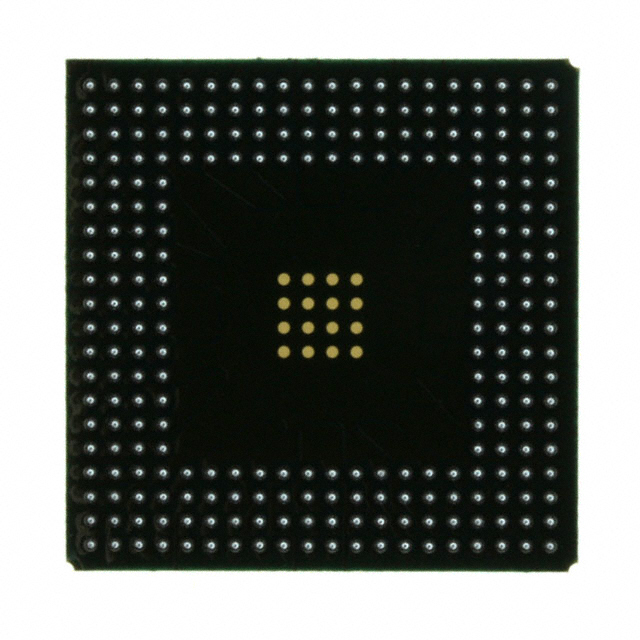
XCV50-6PQ240C
| Part Description |
Virtex® Field Programmable Gate Array (FPGA) IC 166 32768 1728 240-BFQFP |
|---|---|
| Quantity | 506 Available (as of June 14, 2026) |

| Product Category | Field Programmable Gate Array (FPGA) |
|---|---|
| Manufacturer | AMD |
| Manufacturing Status | Obsolete |
| Manufacturer Standard Lead Time | Contact Us |
| Datasheet |
Specifications & Environmental
| Device Package | 240-PQFP (32x32) | Grade | Commercial | Operating Temperature | 0°C – 85°C | ||
|---|---|---|---|---|---|---|---|
| Package / Case | 240-BFQFP | Number of I/O | 166 | Voltage | 2.375 V - 2.625 V | ||
| Mounting Method | Surface Mount | RoHS Compliance | RoHS non-compliant | REACH Compliance | REACH Unaffected | ||
| Moisture Sensitivity Level | 3 (168 Hours) | Number of LABs/CLBs | 384 | Number of Logic Elements/Cells | 1728 | ||
| Number of Gates | 57906 | ECCN | EAR99 | HTS Code | 8542.39.0001 | ||
| Qualification | N/A | Total RAM Bits | 32768 |
Overview of XCV50-6PQ240C – Virtex® Field Programmable Gate Array (FPGA), 240-BFQFP
The XCV50-6PQ240C is an SRAM-based Virtex FPGA offering 57,906 system gates with 1,728 logic elements and approximately 32,768 bits of embedded block RAM. Packaged in a 240-BFQFP surface-mount package, it provides 166 user I/O and operates from a 2.375 V to 2.625 V supply across a commercial temperature range (0 °C to 85 °C).
Designed for fast, high-density programmable logic applications, this device integrates configurable logic, flexible on-chip memory, multi-standard I/O capability and built-in clock management while supporting in-system, reprogrammable configuration.
Key Features
- Core Logic — 1,728 logic elements and 57,906 system gates to implement medium-density programmable logic designs.
- On-chip Memory — Approximately 32,768 bits of block RAM; LUTs are configurable as 16-bit/32-bit RAM, dual-ported RAM, or shift registers as described in the device family architecture.
- I/O and Interface Flexibility — 166 user I/O pins with multi-standard SelectIO™ support and direct connectivity options to high-performance external RAM devices.
- Clock Management — Built-in clock-management circuitry including four dedicated delay-locked loops (DLLs), four primary low-skew global clock nets and 24 secondary local clock nets for refined clock control.
- Configuration and Reprogrammability — SRAM-based in-system configuration with unlimited re-programmability and four programming modes for flexible deployment.
- Process and Reliability — Implemented in a 0.22 µm, 5-layer-metal CMOS process and 100% factory tested for production confidence.
- Package and Mounting — Surface-mount 240-BFQFP (supplier device package: 240-PQFP 32×32) for compact board-level integration.
- Power and Temperature — Operates from 2.375 V to 2.625 V and specified for commercial grade use across 0 °C to 85 °C.
- Compliance — RoHS compliant.
- Development Ecosystem — Supported by FPGA Foundation™ and Alliance Series™ development systems for design implementation and tooling support.
Typical Applications
- PCI and CompactPCI systems — 66-MHz PCI compliance and hot-swap capability (family feature) make the device suitable for PCI-based interface logic and CompactPCI implementations.
- Custom logic / ASIC replacement — Medium-density programmable logic for replacing mask-programmed gate arrays or implementing custom glue logic and control functions.
- Memory interface and bridging — Fast interfaces to external high-performance RAMs and direct connectivity to compatible RAM devices enable memory controller and bridge designs.
- Clock-critical digital systems — On-chip DLLs and multiple clock distribution nets support applications requiring controlled clocking and low-skew timing domains.
Unique Advantages
- Reprogrammable in-system — SRAM-based configuration with unlimited re-programmability simplifies iterative development and field updates without hardware replacement.
- Integrated clock control — Four DLLs and hierarchical clock nets provide precise timing control, reducing external clocking complexity.
- Balanced logic and memory — 1,728 logic elements paired with ~32k bits of block RAM support mixed compute-and-buffer tasks on a single device.
- Compact package with extensive I/O — 166 user I/O in a 240-BFQFP package enables dense interfacing in space-constrained designs.
- Proven process and test coverage — 0.22 µm, 5-layer-metal process and 100% factory testing provide manufacturing consistency.
- Toolchain support — Compatibility with the vendor’s Foundation and Alliance development systems aids design portability and reduces toolchain ramp time.
Why Choose XCV50-6PQ240C?
The XCV50-6PQ240C positions itself as a medium-density, SRAM-based Virtex FPGA that combines a substantive gate count, a practical amount of embedded RAM, and a large complement of I/O in a 240-pin BFQFP package. Its family-level features—multi-standard I/O, on-chip clock management, configurable LUT-based RAM, and in-system reprogrammability—make it well suited to designs that need field-updatable logic, flexible memory configurations, and controlled clock domains.
This device is aimed at designers and teams implementing PCI/CompactPCI interfaces, memory interface logic, or custom programmable logic replacements where proven process technology, tooling support, and production test coverage contribute to predictable integration and long-term maintainability.
Request a quote or submit an inquiry for pricing and availability on the XCV50-6PQ240C to begin evaluating this Virtex FPGA for your design needs.


Date Founded: 1969
Headquarters: Santa Clara, California, USA
Employees: 25,000+
Revenue: $22.68 Billion
Certifications and Memberships: ISO9001:2015, RoHS, REACH


