
XCV50-6FG256C
| Part Description |
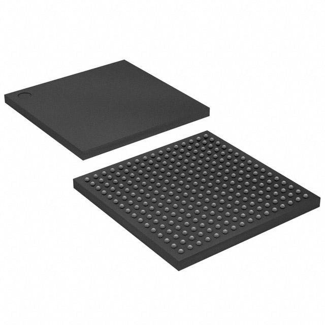
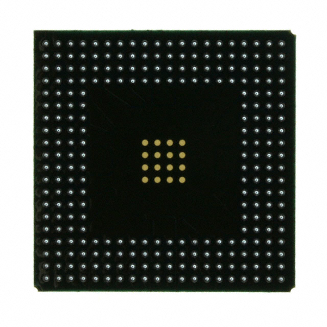
Virtex® Field Programmable Gate Array (FPGA) IC 176 32768 1728 256-BGA |
|---|---|
| Quantity | 974 Available (as of June 10, 2026) |
| Product Category | Field Programmable Gate Array (FPGA) |
|---|---|
| Manufacturer | AMD |
| Manufacturing Status | Obsolete |
| Manufacturer Standard Lead Time | Contact Us |
| Datasheet |
Specifications & Environmental
| Device Package | 256-FBGA (17x17) | Grade | Commercial | Operating Temperature | 0°C – 85°C | ||
|---|---|---|---|---|---|---|---|
| Package / Case | 256-BGA | Number of I/O | 176 | Voltage | 2.375 V - 2.625 V | ||
| Mounting Method | Surface Mount | RoHS Compliance | RoHS non-compliant | REACH Compliance | REACH Unaffected | ||
| Moisture Sensitivity Level | 3 (168 Hours) | Number of LABs/CLBs | 384 | Number of Logic Elements/Cells | 1728 | ||
| Number of Gates | 57906 | ECCN | EAR99 | HTS Code | 8542.39.0001 | ||
| Qualification | N/A | Total RAM Bits | 32768 |
Overview of XCV50-6FG256C – Virtex® Field Programmable Gate Array (FPGA) IC, 176 I/O, 32,768-bit RAM, 1,728 logic elements, 256-BGA
The XCV50-6FG256C is an SRAM-based Virtex FPGA device offering a balance of programmable logic capacity and system I/O for commercial embedded designs. The device integrates approximately 57,906 system gates and 1,728 logic elements with 32,768 bits of embedded RAM to support custom logic, high-performance interfaces and in-system reprogrammability.
Built for configurable system-level applications, the device provides multi-standard I/O, dedicated clock-management resources and on-chip memory options, making it suitable for designs requiring flexible I/O, programmable logic and iterative development cycles.
Key Features
- Core logic — 1,728 logic elements (CLB array 16×24) and approximately 57,906 system gates provide the programmable fabric for custom digital logic and control functions.
- Embedded memory — 32,768 total RAM bits; LUTs configurable as 16-bit/32-bit RAM, dual-ported RAM and shift registers; configurable synchronous dual-ported 4k-bit RAMs for on-chip storage and buffering.
- I/O and interfaces — 176 user I/Os with Multi-standard SelectIO support (16 high-performance interface standards); direct connection capability to ZBTRAM devices; 66‑MHz PCI compliance and hot-swappable support for Compact PCI.
- Clock management — Four dedicated delay-locked loops (DLLs), four primary low-skew global clock nets and 24 secondary local clock nets for advanced clock distribution and low-skew system timing.
- Arithmetic and routing resources — Dedicated carry logic and multiplier support, cascade chains for wide-input functions, abundant registers/latches with clock enable and synchronous/asynchronous control, plus internal 3-state bussing.
- Configuration and re-programmability — SRAM-based in-system configuration with unlimited re-programmability and multiple programming modes (including SelectMAP, serial and JTAG modes).
- Package, power and thermal — 256-ball FBGA package (256-FBGA, 17×17), surface-mount device, supply voltage range 2.375 V to 2.625 V, commercial operating temperature 0 °C to 85 °C, RoHS compliant.
- Process and quality — 0.22 μm, 5-layer-metal CMOS process and 100% factory-tested devices.
Typical Applications
- PCI and Compact PCI systems — Implements custom logic and protocol bridging for 66 MHz PCI-compliant boards and hot-swappable Compact PCI modules.
- Custom embedded systems — Provides programmable logic and on-chip memory for control, glue logic and iterative development in commercial embedded products.
- High-speed memory interfaces — On-chip SelectRAM and fast external RAM interfaces support designs that require tight coupling to external memory.
- Multi-standard I/O bridging — Multi-standard SelectIO and abundant I/O allow interfacing across diverse signaling standards and external devices.
Unique Advantages
- Programmable, iterative development: SRAM-based architecture enables unlimited re-programmability for design prototyping and field updates.
- Integrated clock control: Multiple DLLs and hierarchical clock nets simplify low-skew, multi-clock domain designs.
- Flexible on-chip memory: Configurable LUT-based RAM and dedicated block RAM bits reduce external memory requirements for many control and buffering tasks.
- Broad I/O adaptability: Multi-standard SelectIO and 176 user I/Os allow the device to interface with a wide range of peripherals and memory devices.
- Commercial-grade thermal and supply specs: Defined operating range (0 °C to 85 °C) and narrow core supply range (2.375 V–2.625 V) simplify power and thermal planning for commercial products.
- Proven manufacturing process: 0.22 μm, 5-layer-metal process and 100% factory testing provide traceable device quality for production designs.
Why Choose XCV50-6FG256C?
The XCV50-6FG256C positions itself as a versatile, commercially graded FPGA for designers needing reprogrammable logic, flexible I/O and on-chip memory in a single, surface-mount 256-FBGA package. Its combination of logic elements, embedded RAM and multi-standard I/O supports a range of system-level functions while enabling in-system updates and iterative development.
Backed by support for established FPGA development flows and configuration modes, the device is suited to engineering teams developing PCI/Compact PCI modules, custom embedded controllers and interface bridging solutions that require a programmable, reconfigurable hardware foundation.
Request a quote or submit a purchase inquiry to check pricing and availability for XCV50-6FG256C.


Date Founded: 1969
Headquarters: Santa Clara, California, USA
Employees: 25,000+
Revenue: $22.68 Billion
Certifications and Memberships: ISO9001:2015, RoHS, REACH


