
XCV50-5TQ144I
| Part Description |
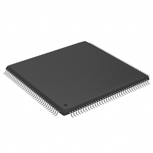
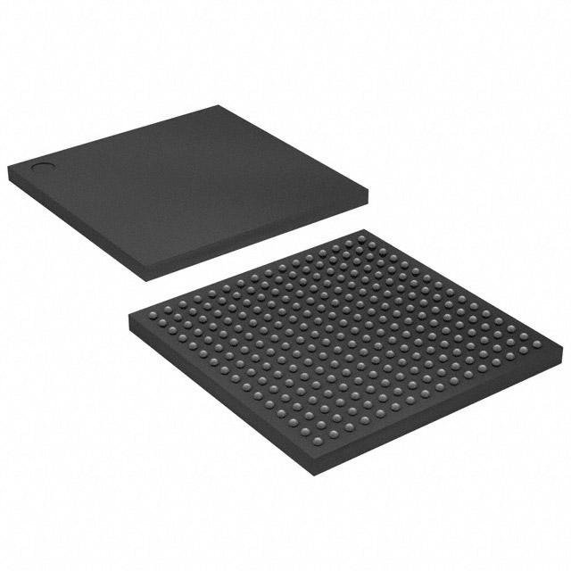
Virtex® Field Programmable Gate Array (FPGA) IC 98 32768 1728 144-LQFP |
|---|---|
| Quantity | 92 Available (as of October 8, 2026) |
| Product Category | Field Programmable Gate Array (FPGA) |
|---|---|
| Manufacturer | AMD |
| Manufacturing Status | Obsolete |
| Manufacturer Standard Lead Time | Contact Us |
| Datasheet |
Specifications & Environmental
| Device Package | 144-TQFP (20x20) | Grade | Industrial | Operating Temperature | -40°C – 100°C | ||
|---|---|---|---|---|---|---|---|
| Package / Case | 144-LQFP | Number of I/O | 98 | Voltage | 2.375 V - 2.625 V | ||
| Mounting Method | Surface Mount | RoHS Compliance | RoHS non-compliant | REACH Compliance | REACH Unaffected | ||
| Moisture Sensitivity Level | 3 (168 Hours) | Number of LABs/CLBs | 384 | Number of Logic Elements/Cells | 1728 | ||
| Number of Gates | 57906 | ECCN | EAR99 | HTS Code | 8542.39.0001 | ||
| Qualification | N/A | Total RAM Bits | 32768 |
Overview of XCV50-5TQ144I – Virtex FPGA, 1728 logic elements, 144-LQFP
The XCV50-5TQ144I is a Virtex® Field Programmable Gate Array (FPGA) optimized for high-performance, reprogrammable digital logic. It provides a flexible SRAM-based architecture with 1,728 logic elements and approximately 32,768 bits of embedded RAM for compact, high-density designs.
Designed for systems that require fast, configurable logic and robust clock management, this device supports common system interfaces and in-system reconfiguration, making it suitable for PCI-class systems, Compact PCI hot-swap applications, and designs that replace mask-programmed gate arrays.
Key Features
- Logic Capacity — 1,728 logic elements and approximately 57,906 system gates provide a compact programmable fabric for mid-density designs.
- Embedded Memory — 32,768 total RAM bits (approximately 0.033 Mbits) with configurable LUT-based RAM and selectable dual-ported RAM modes.
- I/O & Interfaces — 98 available I/O pins with multi-standard SelectIO™ support and compatibility with external high-performance RAM devices.
- Clock Management — Built-in clock-management circuitry including four dedicated DLLs, four primary low-skew global clocks, and multiple secondary local clock nets for advanced timing control.
- Arithmetic & Logic Support — Dedicated carry logic, multiplier support, and cascade chains to accelerate high-speed arithmetic and wide-input functions.
- Configuration & Reprogrammability — SRAM-based in-system configuration with unlimited re-programmability and four programming modes (SelectMAP™, serial, JTAG, etc.).
- Physical & Electrical — Surface-mount 144-LQFP package (supplier package 144-TQFP 20×20) with supply voltage range of 2.375 V to 2.625 V and operating temperature range of −40 °C to 100 °C.
- Process & Quality — Implemented in a 0.22 μm, 5-layer-metal process and 100% factory tested; RoHS compliant.
Typical Applications
- PCI and Compact PCI Systems — Supports 66-MHz PCI compatibility and hot-swappable operation for Compact PCI system designs that require reconfigurable interfaces.
- Custom Logic Replacement — Suitable as a reprogrammable alternative to mask-programmed gate arrays for mid-density logic functions and prototype-to-production workflows.
- Memory Interface Designs — Fast interfaces to external high-performance RAM make it useful for designs that require tight coupling with off-chip memory.
- Clock-Dependent Systems — Devices requiring advanced clock distribution and timing control can leverage the multiple DLLs and global/local clock nets.
- In-System Reconfigurable Designs — SRAM-based configuration and multiple programming modes enable field updates and iterative development cycles.
Unique Advantages
- Balanced Density and Performance: With 1,728 logic elements and roughly 57,906 system gates, the device provides a practical balance of capacity and speed for mid-range FPGA applications.
- Compact Embedded Memory: Approximately 0.033 Mbits of on-chip RAM with configurable LUT and dual-ported options supports a variety of local buffering and small-memory functions.
- Robust Clocking: Multiple DLLs and hierarchical clock distribution reduce clock skew and simplify timing management for synchronous designs.
- Flexible I/O Options: 98 I/Os and multi-standard SelectIO capabilities enable interfacing with a range of external devices and memory technologies.
- Field Reprogrammability: SRAM-based architecture with four programming modes allows in-system updates and iterative design evolution without hardware replacement.
- Industrial Temperature Range & RoHS Compliance: Operation from −40 °C to 100 °C and RoHS compliance support deployment in industrial environments.
Why Choose XCV50-5TQ144I?
The XCV50-5TQ144I is positioned for engineers who need a mid-density, reprogrammable logic device with integrated memory, strong clock management, and flexible I/O. Its feature set—SRAM-based configuration, dedicated arithmetic resources, and DLLs—supports designs that require deterministic timing and the ability to iterate in-system.
For teams developing PCI/Compact PCI systems, memory-interfacing applications, or replacing mask-programmed logic with a reprogrammable solution, this Virtex FPGA delivers a verified manufacturing process and industry-oriented operating range to support robust development and deployment.
Request a quote or submit your procurement inquiry today to check availability and lead time for the XCV50-5TQ144I.





















Date Founded: 1969
Headquarters: Santa Clara, California, USA
Employees: 25,000+
Revenue: $22.68 Billion
Certifications and Memberships: ISO9001:2015, RoHS, REACH











