
XCV50-5FG256I
| Part Description |
Virtex® Field Programmable Gate Array (FPGA) IC 176 32768 1728 256-BGA |
|---|---|
| Quantity | 263 Available (as of June 10, 2026) |
| Product Category | Field Programmable Gate Array (FPGA) |
|---|---|
| Manufacturer | AMD |
| Manufacturing Status | Obsolete |
| Manufacturer Standard Lead Time | Contact Us |
| Datasheet |
Specifications & Environmental
| Device Package | 256-FBGA (17x17) | Grade | Industrial | Operating Temperature | -40°C – 100°C | ||
|---|---|---|---|---|---|---|---|
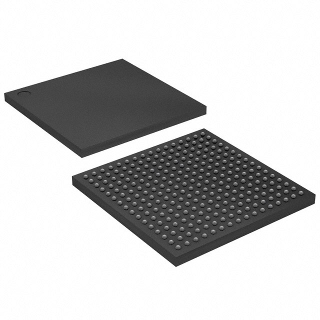
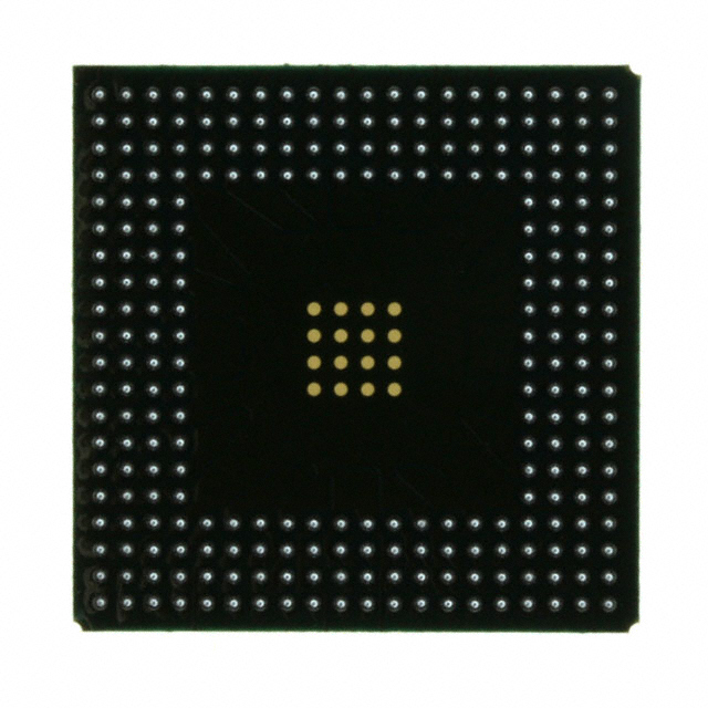
| Package / Case | 256-BGA | Number of I/O | 176 | Voltage | 2.375 V - 2.625 V | ||
| Mounting Method | Surface Mount | RoHS Compliance | RoHS non-compliant | REACH Compliance | REACH Unaffected | ||
| Moisture Sensitivity Level | 3 (168 Hours) | Number of LABs/CLBs | 384 | Number of Logic Elements/Cells | 1728 | ||
| Number of Gates | 57906 | ECCN | EAR99 | HTS Code | 8542.39.0001 | ||
| Qualification | N/A | Total RAM Bits | 32768 |
Overview of XCV50-5FG256I – Virtex® FPGA, 1,728 logic elements, 32,768-bit embedded RAM, 256‑BGA
The XCV50-5FG256I is a Virtex® SRAM-based Field Programmable Gate Array (FPGA) in a 256‑BGA package designed for industrial applications. It integrates a flexible array of configurable logic, on-chip memory, and a high I/O count to enable custom digital logic, interface bridging, and reconfigurable system functions.
Built on the Virtex architecture, this device targets designs that require in-system re-programmability, multi-standard I/O support, and dedicated clock-management resources to balance performance and integration in compact board layouts.
Key Features
- Logic Resources — 1,728 logic elements organized in a CLB array; the datasheet lists a 16 × 24 CLB array (384 CLBs) to support a variety of custom logic implementations.
- On-chip Memory — 32,768 total RAM bits of embedded memory for LUT-based and block RAM storage and buffering directly inside the FPGA fabric.
- I/O and Interfaces — 176 user I/O pins to support multiple external devices and high-pin-count interfaces for system connectivity.
- Clock Management — Dedicated delay-locked loops (DLLs) and multiple global and local clock nets provide advanced clock control for synchronous designs (four DLLs and four primary low-skew global clock distribution nets plus secondary local clock nets as described in the product family documentation).
- Programmability and Configuration — SRAM-based in-system configuration with unlimited re-programmability and multiple programming modes for field updates.
- Package and Mounting — 256‑FBGA (17 × 17) surface-mount package optimized for compact board layouts.
- Electrical and Environmental — Core supply range 2.375 V to 2.625 V; industrial operating temperature range from −40 °C to 100 °C.
- Manufacturing and Quality — 100% factory tested and RoHS compliant.
Typical Applications
- PCI and Compact PCI Systems — Use the device’s interface capabilities and reconfigurability for PCI-compliant and hot-swappable Compact PCI designs, as supported by the Virtex family documentation.
- High-performance Logic Prototyping — Implement custom arithmetic, control, and glue-logic in prototype and low-to-medium volume systems leveraging the device’s dedicated carry logic and multiplier support described in the product family materials.
- Memory Interface and Bridging — Fast interfaces to external high-performance RAMs and configurable LUTs allow use as a memory buffering or interface bridge component.
- Field-reconfigurable Industrial Systems — Industrial-grade temperature range and in-system reprogrammability enable field updates and iterative feature upgrades in industrial control and automated equipment.
Unique Advantages
- Flexible, SRAM-based Re-programmability: Unlimited in-system re-programmability supports iterative development and field updates without hardware replacement.
- Integrated Clock Management: Multiple DLLs and hierarchical clock distribution provide designers with fine-grained timing control for synchronous systems.
- Compact, High-density Package: 256‑FBGA (17 × 17) package enables high integration in space-constrained board designs.
- Industrial Temperature Range: Rated −40 °C to 100 °C to meet demanding environmental requirements for industrial deployments.
- Substantial On-chip Memory and Logic: 32,768 bits of embedded RAM combined with 1,728 logic elements and ~57,906 system gates supports mid-density logic and buffering tasks.
- Broad Development Ecosystem: The Virtex family is supported by established Foundation and Alliance development systems referenced in the product documentation, aiding toolchain integration and design flow.
Why Choose XCV50-5FG256I?
The XCV50-5FG256I provides a balanced combination of configurable logic, embedded memory, and advanced clocking features in an industrial-grade package. It is suited to designers who need a reprogrammable mid-density FPGA with substantial I/O, deterministic clock resources, and on-chip RAM for control, interface, and prototyping applications.
Its support for in-system configuration and the broader Virtex development ecosystem delivers long-term design flexibility and the ability to iterate features in the field, helping to reduce time-to-market and simplify system upgrades.
Request a quote or submit an inquiry to evaluate XCV50-5FG256I for your next reconfigurable logic design project.


Date Founded: 1969
Headquarters: Santa Clara, California, USA
Employees: 25,000+
Revenue: $22.68 Billion
Certifications and Memberships: ISO9001:2015, RoHS, REACH


