
XCV50-5FG256C
| Part Description |
Virtex® Field Programmable Gate Array (FPGA) IC 176 32768 1728 256-BGA |
|---|---|
| Quantity | 1,631 Available (as of June 15, 2026) |

| Product Category | Field Programmable Gate Array (FPGA) |
|---|---|
| Manufacturer | AMD |
| Manufacturing Status | Obsolete |
| Manufacturer Standard Lead Time | Contact Us |
| Datasheet |
Specifications & Environmental
| Device Package | 256-FBGA (17x17) | Grade | Commercial | Operating Temperature | 0°C – 85°C | ||
|---|---|---|---|---|---|---|---|
| Package / Case | 256-BGA | Number of I/O | 176 | Voltage | 2.375 V - 2.625 V | ||
| Mounting Method | Surface Mount | RoHS Compliance | RoHS non-compliant | REACH Compliance | REACH Unaffected | ||
| Moisture Sensitivity Level | 3 (168 Hours) | Number of LABs/CLBs | 384 | Number of Logic Elements/Cells | 1728 | ||
| Number of Gates | 57906 | ECCN | EAR99 | HTS Code | 8542.39.0001 | ||
| Qualification | N/A | Total RAM Bits | 32768 |
Overview of XCV50-5FG256C – Virtex® Field Programmable Gate Array (FPGA) IC, 176 I/O, 32,768-bit RAM, 1,728 logic elements, 256-BGA
The XCV50-5FG256C is a Virtex® SRAM-based Field Programmable Gate Array designed for mid-range programmable logic applications. Its architecture blends configurable logic, embedded memory, and a rich I/O fabric to support high-performance custom digital designs.
Targeted at designers who need reprogrammable, high-density logic—together with flexible I/O and clock management—the device is supplied in a 256-pin BGA package and is suitable for commercial-temperature applications.
Key Features
- Logic Capacity: 1,728 logic elements supporting complex combinational and sequential logic implementations; approximately 57,906 system gates as specified.
- Embedded Memory: Approximately 0.033 Mbits of embedded RAM (32,768 bits) for on-chip data storage and buffer requirements.
- I/O Resources: 176 user I/O pins to support a broad range of external interfaces and system connectivity.
- Clock Management: Four dedicated delay-locked loops (DLLs), four primary low‑skew global clock distribution nets and 24 secondary local clock nets for advanced clock control and low-skew distribution.
- High-performance Interfaces: Multi-standard SelectIO™ support (multiple high-performance interface standards) and fast external memory interfaces as described in the Virtex family specification.
- Arithmetic and DSP Support: Dedicated carry logic and multiplier support for accelerated arithmetic and DSP functions.
- Configuration and Re-programmability: SRAM-based in-system configuration with unlimited re-programmability and multiple programming modes (including SelectMAP™, master/slave serial and JTAG modes).
- Process and Quality: Manufactured on a 0.22 μm 5-layer-metal process and 100% factory tested.
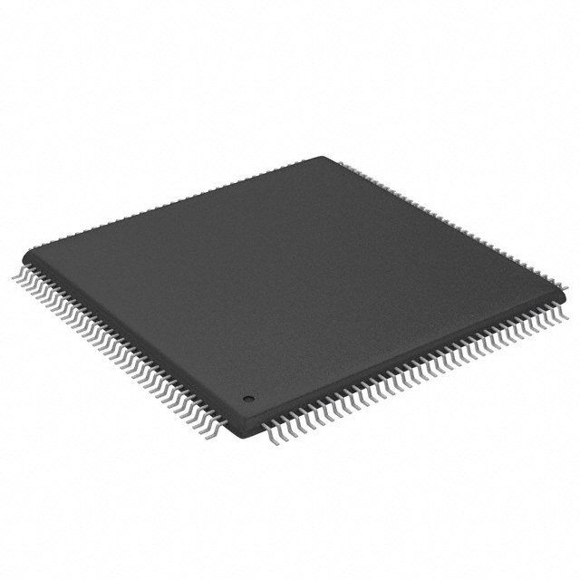
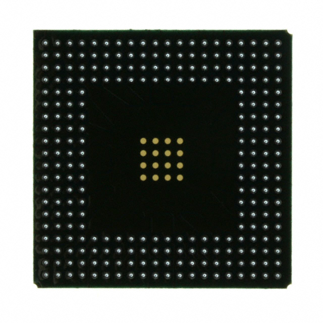
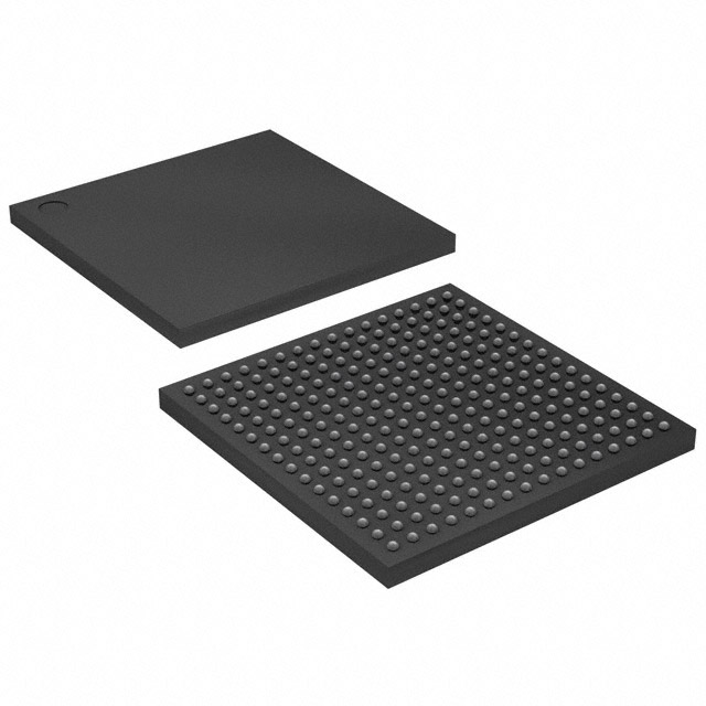
- Package & Mounting: 256-BGA (supplier package: 256-FBGA, 17×17), surface-mount package for board-level assembly.
- Electrical & Environmental: Core supply voltage range 2.375 V to 2.625 V; commercial operating temperature range 0 °C to 85 °C. RoHS compliant.
Typical Applications
- PCI and CompactPCI systems: The device supports PCI-compliant operation and hot‑swappability for CompactPCI-based implementations as specified for devices in the Virtex family.
- High-performance interface bridging: With abundant I/O and SelectIO capabilities, use this FPGA to implement protocol translation and custom high-speed interface logic.
- Custom digital processing and control: Ideal for mid-range custom logic, control functions, and prototype designs that benefit from in-system reprogramming.
Unique Advantages
- Balanced performance and density: Provides a mix of logic elements, embedded RAM, and I/O that fits mid-range programmable logic needs without over-specifying system resources.
- Advanced clocking resources: Four DLLs and multiple global/local clock nets enable precise clock distribution for timing-critical designs.
- Flexible in-system configuration: SRAM-based architecture with multiple programming modes permits rapid iteration and field updates.
- Dedicated arithmetic support: Built-in carry chains and multiplier support reduce implementation complexity for arithmetic-intensive functions.
- Proven manufacturing process: Fabricated on a 0.22 μm 5-layer-metal process and subjected to 100% factory testing for predictable supply quality.
Why Choose XCV50-5FG256C?
The XCV50-5FG256C delivers a compact, reprogrammable FPGA solution that combines configurable logic, embedded memory, and comprehensive I/O in a 256-BGA package. Its Virtex architecture provides clock-management features, dedicated arithmetic support, and multi-standard I/O to help reduce design complexity for mid-range applications.
This device is well suited to engineers and teams needing a commercially graded FPGA with established development tool support and multiple in-system configuration modes, offering long-term design flexibility through unlimited re-programmability.
Request a quote or submit an RFQ to get pricing, availability, and procurement options for the XCV50-5FG256C. Provide your quantity and delivery requirements to receive a prompt response.


Date Founded: 1969
Headquarters: Santa Clara, California, USA
Employees: 25,000+
Revenue: $22.68 Billion
Certifications and Memberships: ISO9001:2015, RoHS, REACH


