
XCV50-5CS144C
| Part Description |
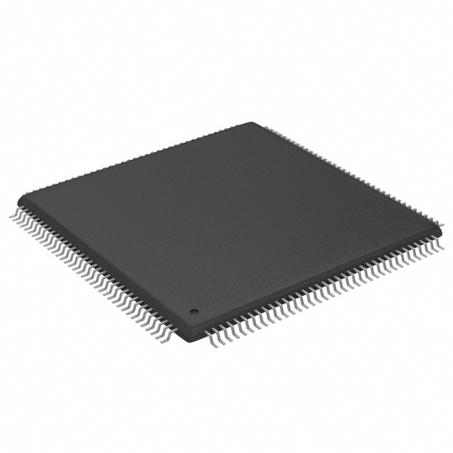
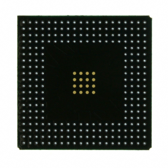
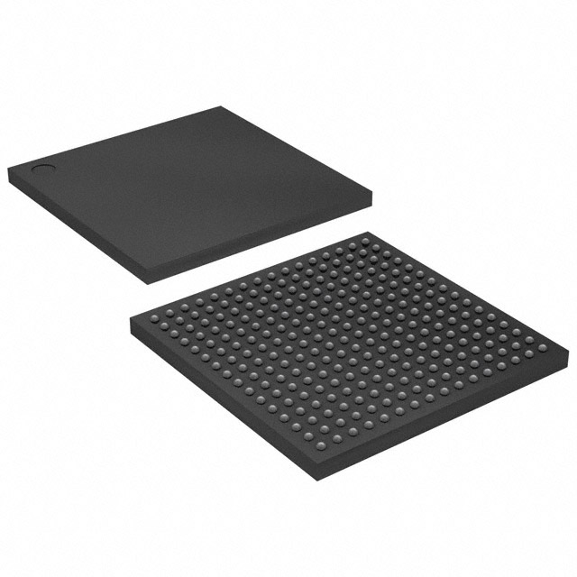
Virtex® Field Programmable Gate Array (FPGA) IC 94 32768 1728 144-TFBGA, CSPBGA |
|---|---|
| Quantity | 1,296 Available (as of June 10, 2026) |

| Product Category | Field Programmable Gate Array (FPGA) |
|---|---|
| Manufacturer | AMD |
| Manufacturing Status | Obsolete |
| Manufacturer Standard Lead Time | Contact Us |
| Datasheet |
Specifications & Environmental
| Device Package | 144-LCSBGA (12x12) | Grade | Commercial | Operating Temperature | 0°C – 85°C | ||
|---|---|---|---|---|---|---|---|
| Package / Case | 144-TFBGA, CSPBGA | Number of I/O | 94 | Voltage | 2.375 V - 2.625 V | ||
| Mounting Method | Surface Mount | RoHS Compliance | RoHS non-compliant | REACH Compliance | REACH Unaffected | ||
| Moisture Sensitivity Level | 3 (168 Hours) | Number of LABs/CLBs | 384 | Number of Logic Elements/Cells | 1728 | ||
| Number of Gates | 57906 | ECCN | EAR99 | HTS Code | 8542.39.0001 | ||
| Qualification | N/A | Total RAM Bits | 32768 |
Overview of XCV50-5CS144C – Virtex Field Programmable Gate Array (FPGA)
The XCV50-5CS144C is an SRAM-based Virtex FPGA offering re-programmable, high-density programmable logic in a compact 144-TFBGA (CSPBGA) surface-mount package. It delivers a balance of logic capacity, on-chip memory, and I/O count suited for system designs that require flexible, in-system reprogrammability and integrated clock and I/O management.
Built on the Virtex architecture, this device targets applications that need configurable logic, embedded RAM, and multi-standard I/O support, while operating within a commercial temperature range and a 2.375 V to 2.625 V core supply window.
Key Features
- Logic Capacity — 1,728 logic elements and approximately 57,906 system gates provide programmable combinational and sequential logic resources for custom digital designs.
- Embedded Memory — 32,768 bits of on-chip RAM (block RAM) plus configurable LUT-based RAM options for flexible data storage and buffering.
- I/O — 94 user I/O pins to support a variety of external interfaces and peripherals.
- Clock Management — Built-in clock-management circuitry from the Virtex family, including four dedicated DLLs and multiple global and local clock nets for advanced clock distribution and low-skew operation.
- Programmable Logic Architecture — Features such as dedicated carry logic, multiplier support, cascade chains, abundant registers with clock-enable and set/reset functionality, and internal 3-state bussing for building arithmetic, DSP, and wide-input functions.
- Configurable LUTs and Block RAM — LUTs that can be configured as various RAM styles (including dual-ported options) and fast, hierarchical memory resources for efficient data-path implementation.
- SRAM-Based In-System Configuration — SRAM configuration supports unlimited re-programmability with multiple configuration modes described in the Virtex family specification.
- Package & Mounting — 144-TFBGA (CSPBGA), surface-mount package (supplier device package: 144-LCSBGA, 12×12) for compact board-level integration.
- Electrical & Environmental — Core voltage range 2.375 V to 2.625 V; commercial operating temperature range 0 °C to 85 °C; RoHS compliant.
Typical Applications
- PCI and Compact PCI systems — Use the device’s high-speed I/O and Virtex family compatibility for PCI-compliant interfaces and hot-swappable Compact PCI designs.
- Custom memory controllers and high-performance buffering — Leverage on-chip block RAM and configurable LUT-based RAM for buffering, queuing, and interfacing to external high-performance RAMs.
- Arithmetic and DSP functions — Implement adders, multipliers, and pipelined arithmetic using dedicated carry logic and multiplier support.
- Reconfigurable system prototyping — Take advantage of SRAM-based in-system configuration for iterative development and field updates.
Unique Advantages
- Re-programmability: SRAM-based configuration enables unlimited re-programmability to refine designs or update functionality in the field.
- Balanced resource set: The combination of ~57.9k system gates, 1,728 logic elements, and 32,768 bits of block RAM supports mid-density designs with integrated memory and logic.
- Integrated clock control: Multiple DLLs and global/local clock distribution resources reduce clock skew and simplify multi-clock-domain designs.
- Compact package: 144-TFBGA (12×12) BGA footprint allows integration into space-constrained PCBs while providing adequate I/O and thermal characteristics for commercial applications.
- Design ecosystem: The Virtex family is supported by FPGA Foundation and Alliance development systems described in the datasheet, enabling standard design flows and tool support.
Why Choose XCV50-5CS144C?
The XCV50-5CS144C offers a practical balance of programmable logic, embedded memory, and I/O in a compact BGA package for commercial-temperature applications. Its Virtex-family clock management, configurable LUTs, and SRAM-based in-system configuration make it well suited for developers who need a re-programmable platform for mid-density digital designs, interface controllers, and custom arithmetic or buffering functions.
With RoHS compliance and support from the Virtex development ecosystem, this device provides predictable electrical and environmental characteristics (2.375 V–2.625 V core, 0 °C–85 °C) and a development path for iterative design and in-field updates.
Request a quote or submit an inquiry to receive pricing and availability information for the XCV50-5CS144C. Our team can provide lead-time details and assist with volume and procurement questions.


Date Founded: 1969
Headquarters: Santa Clara, California, USA
Employees: 25,000+
Revenue: $22.68 Billion
Certifications and Memberships: ISO9001:2015, RoHS, REACH


