
XCV50-5PQ240I
| Part Description |
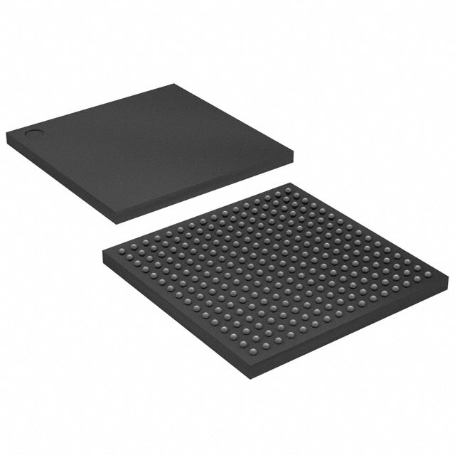
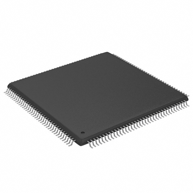
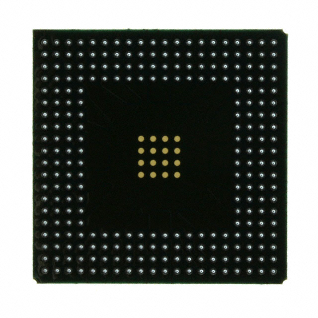
Virtex® Field Programmable Gate Array (FPGA) IC 166 32768 1728 240-BFQFP |
|---|---|
| Quantity | 1,772 Available (as of October 8, 2026) |

| Product Category | Field Programmable Gate Array (FPGA) |
|---|---|
| Manufacturer | AMD |
| Manufacturing Status | Obsolete |
| Manufacturer Standard Lead Time | Contact Us |
| Datasheet |
Specifications & Environmental
| Device Package | 240-PQFP (32x32) | Grade | Industrial | Operating Temperature | -40°C – 100°C | ||
|---|---|---|---|---|---|---|---|
| Package / Case | 240-BFQFP | Number of I/O | 166 | Voltage | 2.375 V - 2.625 V | ||
| Mounting Method | Surface Mount | RoHS Compliance | RoHS non-compliant | REACH Compliance | REACH Unaffected | ||
| Moisture Sensitivity Level | 3 (168 Hours) | Number of LABs/CLBs | 384 | Number of Logic Elements/Cells | 1728 | ||
| Number of Gates | 57906 | ECCN | EAR99 | HTS Code | 8542.39.0001 | ||
| Qualification | N/A | Total RAM Bits | 32768 |
Overview of XCV50-5PQ240I – Virtex® Field Programmable Gate Array (FPGA) IC 166 32768 1728 240-BFQFP
The XCV50-5PQ240I is a Virtex® SRAM-based FPGA delivering moderate-density programmable logic with 1,728 logic elements, 32,768 bits of on-chip RAM and 166 user I/O. Built on a 0.22 µm, 5-layer metal process and supported by Foundation and Alliance development systems, it targets embedded systems, communications and industrial control designs that require flexible I/O, on-chip memory and configurable clocking.
Designed for surface-mount assembly in a 240-BFQFP (240-PQFP, 32×32) package, the device operates from 2.375 V to 2.625 V and across an industrial temperature range of −40 °C to 100 °C.
Key Features
- Logic Capacity — 1,728 logic elements organized across 384 CLBs (16×24 CLB array) and approximately 57,906 system gates for mid-range programmable logic integration.
- Embedded Memory — 32,768 total RAM bits of on-chip block RAM to support buffering, FIFOs and small data structures without external memory.
- Flexible I/O — 166 user I/O pins with multi-standard SelectIO™ capabilities for diverse interface requirements.
- Clock Management — Four dedicated delay-locked loops (DLLs), four primary low-skew global clock nets and 24 secondary local clock nets for advanced clock distribution and control.
- Configurable Logic — LUTs that can be configured as RAM (16/32-bit), dual-ported RAM or shift registers; dedicated carry logic and multiplier support for arithmetic-intensive functions.
- Configuration and In-System Reprogramming — SRAM-based device with unlimited re-programmability and four programming modes (SelectMAP™, slave serial, master serial, JTAG).
- System Integration — IEEE 1149.1 boundary-scan support, die-temperature sensor diode and internal 3-state bussing to simplify board-level integration and diagnostics.
- Process and Test — Manufactured in a 0.22 µm, 5-layer-metal CMOS process and 100% factory tested for production reliability.
- Package & Temperature — Surface-mount 240-BFQFP package; industrial operating range −40 °C to 100 °C and supply range 2.375 V to 2.625 V.
Typical Applications
- Industrial Control: Implement motion control, protocol bridging and real-time I/O aggregation using on-chip RAM and programmable logic while meeting industrial temperature requirements.
- Communications Equipment: Use the device’s flexible I/O and clock-management resources for interface bridging, packet buffering and timing-critical data paths.
- Embedded System Prototyping: Leverage SRAM-based in-system reprogrammability and Foundation/Alliance tool support to iterate designs quickly and validate hardware/firmware integration.
- Compact PCI / PCI Systems: Support 66‑MHz PCI-compliant interfaces and hot-swappable Compact PCI topologies with the programmable I/O and reconfiguration capabilities.
Unique Advantages
- Balanced Logic and Memory: 1,728 logic elements combined with 32,768 bits of on-chip RAM provide a compact platform for mid-density designs without immediate external memory dependencies.
- Advanced Clocking: Four DLLs and multiple dedicated clock nets enable low-skew distribution and flexible clock domain management for synchronous designs.
- Flexible I/O Integration: 166 user I/Os with SelectIO support allow direct interfacing to a variety of peripherals and external memory devices.
- Reprogrammable SRAM Architecture: Unlimited in-system re-programmability and four configuration modes streamline firmware updates and field revisions.
- Industrial Qualifications: Specified for surface-mount deployment and operation from −40 °C to 100 °C, suitable for a wide range of industrial applications.
- Proven Manufacturing: 0.22 µm, 5-layer-metal process and 100% factory testing support predictable production outcomes.
Why Choose XCV50-5PQ240I?
The XCV50-5PQ240I is positioned for designers who need a moderate-density, reprogrammable FPGA with a balanced mix of logic, embedded RAM and flexible I/O in a compact BFQFP package. Its built-in clock management, configurable LUT memory modes and dedicated arithmetic resources make it well suited to applications that require precise timing, interface flexibility and iterative development.
Backed by Foundation and Alliance development system support and manufactured on a mature CMOS process, the device provides an integrated solution for teams focused on industrial and communications applications that demand on-board memory, programmable logic and in-field configurability.
Request a quote or submit an inquiry to get pricing and availability for the XCV50-5PQ240I. Our team can provide lead times, procurement options and support for your evaluation and production planning.




















Date Founded: 1969
Headquarters: Santa Clara, California, USA
Employees: 25,000+
Revenue: $22.68 Billion
Certifications and Memberships: ISO9001:2015, RoHS, REACH











