
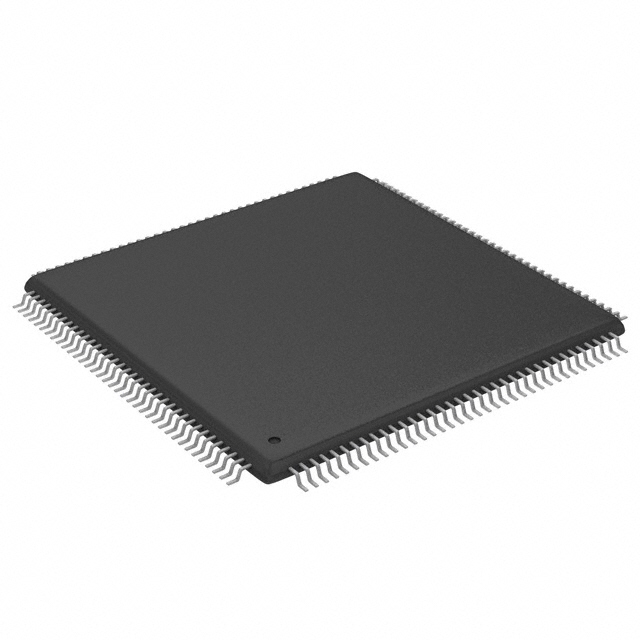
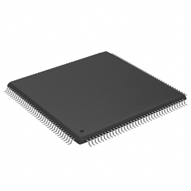
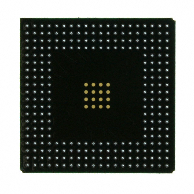
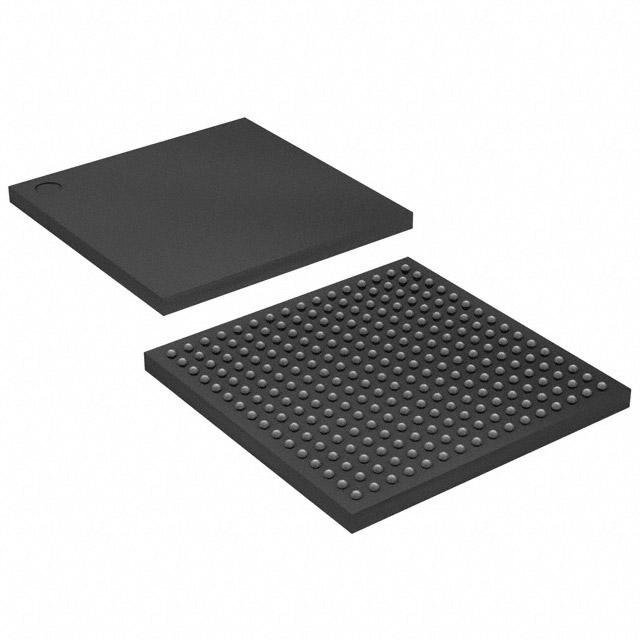
XCV50-6CS144C
| Part Description |
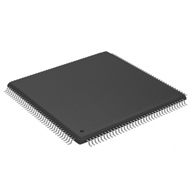
Virtex® Field Programmable Gate Array (FPGA) IC 94 32768 1728 144-TFBGA, CSPBGA |
|---|---|
| Quantity | 763 Available (as of October 8, 2026) |

| Product Category | Field Programmable Gate Array (FPGA) |
|---|---|
| Manufacturer | AMD |
| Manufacturing Status | Obsolete |
| Manufacturer Standard Lead Time | Contact Us |
| Datasheet |
Specifications & Environmental
| Device Package | 144-LCSBGA (12x12) | Grade | Commercial | Operating Temperature | 0°C – 85°C | ||
|---|---|---|---|---|---|---|---|
| Package / Case | 144-TFBGA, CSPBGA | Number of I/O | 94 | Voltage | 2.375 V - 2.625 V | ||
| Mounting Method | Surface Mount | RoHS Compliance | RoHS non-compliant | REACH Compliance | REACH Unaffected | ||
| Moisture Sensitivity Level | 3 (168 Hours) | Number of LABs/CLBs | 384 | Number of Logic Elements/Cells | 1728 | ||
| Number of Gates | 57906 | ECCN | EAR99 | HTS Code | 8542.39.0001 | ||
| Qualification | N/A | Total RAM Bits | 32768 |
Overview of XCV50-6CS144C – Virtex® Field Programmable Gate Array (FPGA) IC, 144-TFBGA
The XCV50-6CS144C is an SRAM-based Virtex® FPGA offered in a 144-TFBGA (CSPBGA) surface-mount package. It provides 1,728 logic elements, approximately 32,768 bits of on-chip RAM, and 94 user I/O, making it suitable for commercial-grade programmable-logic designs requiring reprogrammability and flexible I/O.
As a member of the Virtex family, this device benefits from the architecture and tool support associated with the series, including hierarchical memory options and integrated clock-management resources that address a range of system-level and board-level integration needs.
Key Features
- Logic Capacity 1,728 logic elements and a device gate count of 57,906 enable mid-range programmable logic implementations.
- On-Chip Memory Approximately 32,768 bits of embedded RAM for local data storage and small buffers.
- I/O Resources 94 user I/O pins provided in the 144-TFBGA package for board-level connectivity and external peripheral interfacing.
- Clock and Timing Virtex family clock-management features such as dedicated delay-locked loops (DLLs) and hierarchical global/local clock nets are available for advanced clock control and low-skew distribution.
- Architecture Features Family-level architecture includes dedicated carry logic, multiplier support, cascade chains for wide functions, abundant registers with clock enable, internal 3-state bussing, and IEEE 1149.1 boundary-scan support.
- Configuration and Re-programmability SRAM-based in-system configuration provides unlimited re-programmability and multiple programming modes supported by the Virtex family.
- Package and Mounting Surface-mount 144-TFBGA (supplier package 144-LCSBGA 12×12) for compact board placement and high-density designs.
- Power and Temperature Supply voltage range 2.375 V to 2.625 V with an operating temperature range of 0 °C to 85 °C, suitable for commercial-grade applications.
- Quality and Compliance 100% factory tested and RoHS compliant as documented for the device family.
Typical Applications
- PCI and Compact PCI Systems Family documentation identifies PCI-capable performance and hot-swappable support for Compact PCI—useful for board-level I/O subsystems and legacy PCI interfaces.
- Embedded and Custom Logic Mid-range logic density and on-chip RAM support embedded control, protocol bridging, and custom peripheral functions.
- Memory Interface and Buffering On-chip RAM plus family-level fast interfaces to external high-performance RAMs make the device suitable for local buffering and temporary data storage.
- Prototyping and In-System Development SRAM-based in-system configuration enables iterative firmware development and reprogramming during design validation and prototyping.
Unique Advantages
- Balanced Logic and Memory: Combines 1,728 logic elements with approximately 32,768 bits of embedded RAM to support both control logic and local data storage on a single device.
- Flexible Clocking: Built-in clock-management circuitry (family-level) simplifies implementation of multiple clock domains and low-skew distribution across the design.
- Compact, Board-Friendly Package: 144-TFBGA surface-mount package with a 12×12 supplier footprint minimizes PCB area while providing substantial I/O count.
- Commercial Temperature Range: Rated 0 °C to 85 °C for designs targeting commercial environments.
- Proven Ecosystem Support: Part of the Virtex family, with documented support from Foundation and Alliance development systems for design flow and configuration options.
- Regulatory and Test Confidence: RoHS compliant and 100% factory tested to support predictable supply-chain and manufacturing integration.
Why Choose XCV50-6CS144C?
The XCV50-6CS144C provides a mid-range Virtex FPGA option that balances logic capacity, embedded RAM, and a compact BGA package for commercial programmable-logic applications. Its SRAM-based configuration and family-level clocking and architecture features make it suitable for designs that require reprogrammability, flexible I/O, and hierarchical memory structures.
This device is well suited to engineers and teams building board-level subsystems, prototyping logic-intensive functions, or integrating configurable interfaces where predictable thermal and voltage specifications (2.375 V–2.625 V, 0 °C–85 °C) and RoHS compliance are required.
If you would like pricing or availability information, request a quote or submit an inquiry to obtain a tailored purchase estimate and lead-time for the XCV50-6CS144C.




















Date Founded: 1969
Headquarters: Santa Clara, California, USA
Employees: 25,000+
Revenue: $22.68 Billion
Certifications and Memberships: ISO9001:2015, RoHS, REACH











