
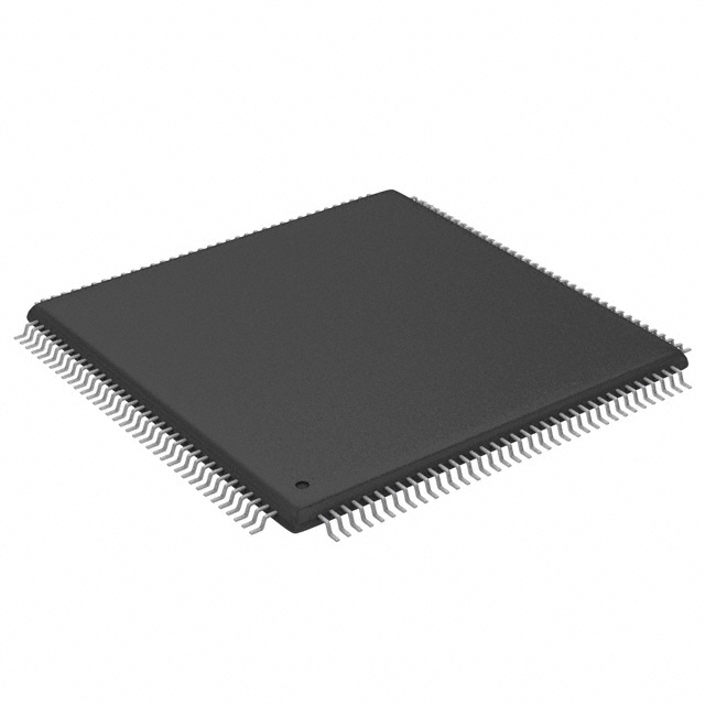
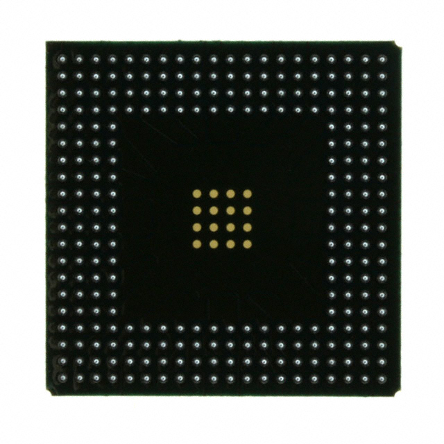
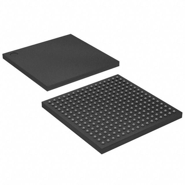
XCV50-6TQ144C
| Part Description |
Virtex® Field Programmable Gate Array (FPGA) IC 98 32768 1728 144-LQFP |
|---|---|
| Quantity | 552 Available (as of June 15, 2026) |
| Product Category | Field Programmable Gate Array (FPGA) |
|---|---|
| Manufacturer | AMD |
| Manufacturing Status | Obsolete |
| Manufacturer Standard Lead Time | Contact Us |
| Datasheet |
Specifications & Environmental
| Device Package | 144-TQFP (20x20) | Grade | Commercial | Operating Temperature | 0°C – 85°C | ||
|---|---|---|---|---|---|---|---|
| Package / Case | 144-LQFP | Number of I/O | 98 | Voltage | 2.375 V - 2.625 V | ||
| Mounting Method | Surface Mount | RoHS Compliance | RoHS non-compliant | REACH Compliance | REACH Unaffected | ||
| Moisture Sensitivity Level | 3 (168 Hours) | Number of LABs/CLBs | 384 | Number of Logic Elements/Cells | 1728 | ||
| Number of Gates | 57906 | ECCN | EAR99 | HTS Code | 8542.39.0001 | ||
| Qualification | N/A | Total RAM Bits | 32768 |
Overview of XCV50-6TQ144C – Virtex Field Programmable Gate Array (FPGA), 98 I/O, 32,768-bit RAM, 1,728 Logic Elements, 144-LQFP
The XCV50-6TQ144C is a Virtex-series SRAM-based Field Programmable Gate Array offering 1,728 logic elements and 32,768 bits of embedded block RAM in a compact 144-LQFP package. Designed for commercial-grade applications, it provides flexible programmable logic, a broad I/O set, and on-chip memory for custom digital functions and system interfacing.
Its architecture supports in-system configuration and a range of clocking and I/O options, making it suitable for medium-density logic integration, PCI-compliant designs, and systems requiring fast external memory interfaces.
Key Features
- Logic Capacity — 1,728 logic elements (configured from the Virtex CLB fabric) with an estimated 57,906 system-gate equivalent for implementing custom combinational and sequential logic.
- On-chip Memory — 32,768 bits of block RAM and support for LUT-configured RAM and shift-register modes provide local storage for buffers, FIFOs, and small data tables.
- I/O and Interface Flexibility — 98 available I/O pins and multi-standard SelectIO™ interfaces enable connection to a variety of external devices; the device documentation notes direct connection capability to ZBTRAM devices and 66-MHz PCI compliance.
- Clocking and Timing — Built-in clock-management resources including four dedicated delay-locked loops (DLLs), four primary low-skew global clock nets, and additional local clock distribution for advanced clock control and low-skew routing.
- Configuration and Reprogrammability — SRAM-based in-system configuration offers unlimited re-programmability with multiple programming modes (SelectMAP™, slave serial, master serial, and JTAG).
- Package and Mounting — 144-LQFP package (supplier device package: 144-TQFP, 20×20) with surface-mount mounting for compact PCB integration.
- Electrical and Environmental — Operating voltage range of 2.375 V to 2.625 V and commercial operating temperature range of 0 °C to 85 °C; RoHS compliant.
Typical Applications
- PCI and Peripheral Interfaces — Implement PCI-compliant logic and custom peripheral bridges leveraging the device’s I/O count and documented 66-MHz PCI compatibility.
- Memory Interface and Buffering — Use the on-chip block RAM and fast external RAM interfaces for buffering, caching, and custom memory controllers.
- Custom Logic and Prototyping — Medium-density programmable logic for prototyping and production designs that require reprogrammability and on-board configurability.
- High-performance I/O Bridging — Multi-standard SelectIO™ and ample I/O allow the FPGA to act as an interface hub between diverse digital components and peripherals.
Unique Advantages
- Reprogrammable SRAM Architecture: Unlimited in-system re-programmability enables iterative development and field updates without hardware changes.
- Balanced Logic and Memory: The combination of 1,728 logic elements and 32,768 bits of embedded RAM supports a wide range of mid-scale digital functions while minimizing external memory needs.
- Advanced Clocking Resources: Four dedicated DLLs and multiple global/local clock nets simplify complex clock-domain implementations and reduce clock skew.
- Compact, Surface-Mount Package: 144-LQFP (144-TQFP 20×20) delivers a small PCB footprint for space-constrained designs.
- Established Development Support: The Virtex family is supported by the FPGA Foundation™ and Alliance development systems for a complete design flow and toolchain compatibility as documented for the series.
Why Choose XCV50-6TQ144C?
The XCV50-6TQ144C provides a balanced mix of programmable logic, embedded memory, and flexible I/O in a commercial-grade, surface-mount package. Its SRAM-based reprogrammability and on-chip clock-management features make it well suited for mid-density custom logic, interface bridging, and systems requiring field-update capability.
Engineers and purchasers looking for a proven Virtex-series FPGA with established tool support and a compact package will find the XCV50-6TQ144C appropriate for designs that need moderate gate density, reliable I/O capacity, and integrated memory resources.
Request a quote or submit an inquiry to check availability and pricing for the XCV50-6TQ144C.


Date Founded: 1969
Headquarters: Santa Clara, California, USA
Employees: 25,000+
Revenue: $22.68 Billion
Certifications and Memberships: ISO9001:2015, RoHS, REACH


