
XCV600-6HQ240C
| Part Description |
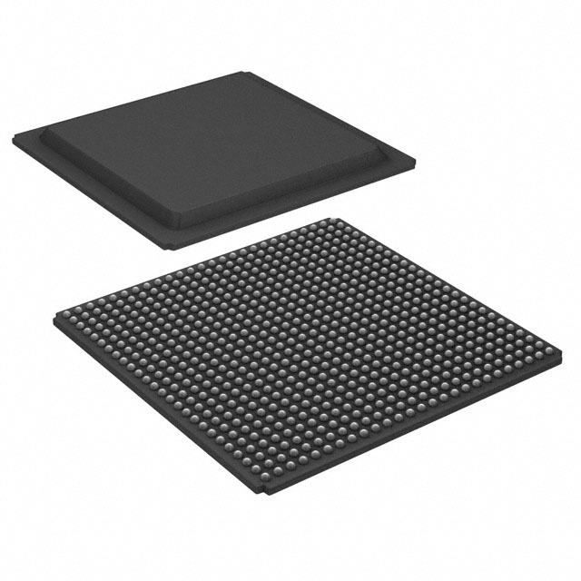
Virtex® Field Programmable Gate Array (FPGA) IC 166 98304 15552 240-BFQFP Exposed Pad |
|---|---|
| Quantity | 368 Available (as of June 15, 2026) |

| Product Category | Field Programmable Gate Array (FPGA) |
|---|---|
| Manufacturer | AMD |
| Manufacturing Status | Obsolete |
| Manufacturer Standard Lead Time | Contact Us |
| Datasheet |
Specifications & Environmental
| Device Package | 240-PQFP (32x32) | Grade | Commercial | Operating Temperature | 0°C – 85°C | ||
|---|---|---|---|---|---|---|---|
| Package / Case | 240-BFQFP Exposed Pad | Number of I/O | 166 | Voltage | 2.375 V - 2.625 V | ||
| Mounting Method | Surface Mount | RoHS Compliance | RoHS non-compliant | REACH Compliance | REACH Unaffected | ||
| Moisture Sensitivity Level | 3 (168 Hours) | Number of LABs/CLBs | 3456 | Number of Logic Elements/Cells | 15552 | ||
| Number of Gates | 661111 | ECCN | 3A001A7B | HTS Code | 8542.39.0001 | ||
| Qualification | N/A | Total RAM Bits | 98304 |
Overview of XCV600-6HQ240C – Virtex® FPGA IC 240-BFQFP Exposed Pad
The XCV600-6HQ240C is an AMD Virtex® field programmable gate array (FPGA) in a 240-BFQFP exposed-pad package intended for commercial applications. It delivers a high-density, SRAM-based programmable logic architecture with on-chip embedded memory and extensive I/O, suited for high-performance system designs and interface-centric applications.
This device supports in-system reprogrammability and a hierarchical memory and clocking architecture, enabling flexible design partitioning and integration for PCI and Compact PCI systems, memory interfaces, and other complex digital subsystems.
Key Features
- Logic Capacity — 15,552 logic elements for implementing complex digital functions and custom logic.
- Configurable Logic Blocks (architecture) — SRAM-based programmable fabric with abundant registers and dedicated carry and multiplier support for arithmetic and wide-input functions.
- Embedded Memory — Approximately 0.098 Mbits of embedded memory (98,304 bits) and configurable LUT-based RAM and SelectRAM+ options for flexible on-chip storage.
- I/O Resources — 166 user I/Os with multi-standard SelectIO™ support and interfaces for external high-performance RAMs and ZBTRAM devices.
- Clock Management — Four dedicated delay-locked loops (DLLs), multiple global and local clock distribution nets for advanced clock control and low-skew distribution.
- Performance and Standards — Designed for high-density, high-performance applications with documented family-level system performance up to 200 MHz and 66-MHz PCI compliance.
- Configuration and Reprogrammability — SRAM-based in-system configuration with multiple programming modes (SelectMAP™, serial, JTAG) and unlimited re-programmability.
- Package and Power — 240-BFQFP exposed-pad (240-PQFP, 32×32) surface-mount package; nominal supply range 2.375 V to 2.625 V.
- Operating Conditions — Commercial grade device with operating temperature range 0 °C to 85 °C and RoHS compliance.
Typical Applications
- PCI and Compact PCI systems — Implements custom interface logic and protocol handling for PCI-compliant designs and hot-swappable Compact PCI subsystems.
- High-performance digital systems — Provides dense programmable fabric and on-chip memory for compute- and throughput-oriented functions in communications and test equipment.
- Memory interface and bridging — Fast interfaces to external high-performance RAMs and support for ZBTRAM connectivity enable memory-intensive designs and buffer management.
- Custom arithmetic and signal processing — Dedicated carry logic and multiplier support simplify implementation of wide arithmetic and DSP-like functions.
Unique Advantages
- High integration density: 15,552 logic elements and abundant embedded memory reduce external component count and simplify system design.
- Flexible I/O and interfacing: 166 user I/Os with multi-standard SelectIO support enable direct connectivity to a wide range of peripherals and memory devices.
- Advanced clocking: Four DLLs and multiple clock distribution nets provide robust options for low-skew, multi-clock designs.
- In-system reprogrammability: SRAM-based configuration with multiple programming modes allows design updates and field reconfiguration without hardware changes.
- Commercial reliability and compliance: Surface-mount 240-BFQFP exposed-pad package and RoHS compliance aid manufacturability and regulatory alignment for commercial products.
Why Choose XCV600-6HQ240C?
The XCV600-6HQ240C positions itself as a versatile, high-density Virtex FPGA option for commercial embedded and system-level designs that require substantial logic capacity, flexible on-chip memory, and extensive I/O. Its SRAM-based architecture and in-system configuration support development agility and field updates.
Designed for engineers building PCI-capable systems, memory interfaces, and compute-focused modules, this device provides a balance of performance, integration, and configurable resources backed by the Virtex family architecture and development ecosystem.
Request a quote or submit a purchase inquiry to check availability and lead times for the XCV600-6HQ240C and to discuss how this device can fit your next design.


Date Founded: 1969
Headquarters: Santa Clara, California, USA
Employees: 25,000+
Revenue: $22.68 Billion
Certifications and Memberships: ISO9001:2015, RoHS, REACH


