
XCV600E-6BG560C
| Part Description |
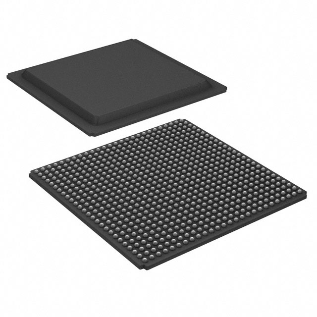
Virtex®-E Field Programmable Gate Array (FPGA) IC 404 294912 15552 560-LBGA Exposed Pad, Metal |
|---|---|
| Quantity | 925 Available (as of June 15, 2026) |

| Product Category | Field Programmable Gate Array (FPGA) |
|---|---|
| Manufacturer | AMD |
| Manufacturing Status | Obsolete |
| Manufacturer Standard Lead Time | Contact Us |
| Datasheet |
Specifications & Environmental
| Device Package | 560-MBGA (42.5x42.5) | Grade | Commercial | Operating Temperature | 0°C – 85°C | ||
|---|---|---|---|---|---|---|---|
| Package / Case | 560-LBGA Exposed Pad, Metal | Number of I/O | 404 | Voltage | 1.71 V - 1.89 V | ||
| Mounting Method | Surface Mount | RoHS Compliance | RoHS non-compliant | REACH Compliance | REACH Unaffected | ||
| Moisture Sensitivity Level | 3 (168 Hours) | Number of LABs/CLBs | 3456 | Number of Logic Elements/Cells | 15552 | ||
| Number of Gates | 985882 | ECCN | 3A991D | HTS Code | 8542.39.0001 | ||
| Qualification | N/A | Total RAM Bits | 294912 |
Overview of XCV600E-6BG560C – Virtex®-E FPGA, 1.8 V, 560-LBGA
The XCV600E-6BG560C is a Virtex®-E Field Programmable Gate Array (FPGA) in a 560-LBGA exposed-pad metal package. It provides a reconfigurable logic fabric with high I/O count and embedded memory suited to designs that require flexible, high-bandwidth interfaces and in-system reprogrammability.
Built on the Virtex-E family architecture, this device targets applications needing substantial on-chip logic and memory capacity combined with a broad set of I/O standards and clock management features. It operates with an internal supply range of 1.71 V to 1.89 V and is specified for commercial temperature operation (0 °C to 85 °C).
Key Features
- Logic Capacity — 15,552 logic elements and approximately 985,882 gates provide a sizeable configurable fabric for medium-to-high density logic implementations.
- Embedded Memory — 294,912 total RAM bits, equivalent to approximately 0.295 Mbits of embedded memory, enabling on-chip buffering and local data storage.
- I/O Density & Flexibility — 404 I/O pins support high-bandwidth external interfaces and system-level connectivity in a compact package.
- High-Performance I/O Standards (series-level) — Virtex‑E SelectI/O+ technology supports a wide range of interface standards and differential signaling (LVDS, BLVDS, LVPECL) for system designs requiring source-synchronous and differential data paths.
- Clock Management (series-level) — Advanced clock management with multiple DLLs enables clock multiplication/division and duty-cycle control for timing-critical applications.
- Memory Hierarchy (series-level) — SelectRAM+ architecture provides distributed RAM and block RAM options to support high bandwidth memory interfaces and true dual-port block RAM functionality.
- Configuration — SRAM-based in-system reconfigurability allows unlimited re-programmability for iterative development and field updates.
- Package & Mounting — 560-LBGA exposed pad, metal package (supplier device package: 560-MBGA, 42.5 × 42.5 mm) and surface-mount mounting type for board-level integration.
- Power and Thermal — Internal supply specified from 1.71 V to 1.89 V; commercial operating temperature range from 0 °C to 85 °C.
- Regulatory — RoHS compliant.
Typical Applications
- High-speed interface controllers — Use the device’s broad I/O support and differential signaling capabilities for designs that require source-synchronous or differential data channels.
- Memory interface and buffering — Leverage the on-chip block and distributed RAM to implement high-performance interfaces to external memories and local buffering.
- PCI-compliant systems — Applicable to designs targeting PCI 3.3 V, 32/64-bit, 33/66-MHz interfaces as supported by the Virtex‑E family.
- Reconfigurable prototyping and system integration — SRAM-based in-system configuration enables iterative development, updates, and flexible system functions.
Unique Advantages
- Substantial logic and gate count: 15,552 logic elements and 985,882 gates provide the resources needed for complex combinational and sequential functions without immediate partitioning across multiple devices.
- High I/O bandwidth: 404 I/O pins allow wide parallel data paths and multiple interfaces on a single device, reducing board-level complexity.
- Embedded memory for local storage: Approximately 0.295 Mbits of on-chip RAM supports buffering, FIFOs, and small embedded datasets close to logic for reduced latency.
- Flexible clocking and interface options: Family-level clock management and SelectI/O+ capabilities enable precise timing control and support for a variety of signaling standards.
- RoHS compliant and surface-mount package: Modern packaging with an exposed pad and metal BGA footprint simplifies thermal management and assembly for commercial designs.
- Re-programmability and development ecosystem (series-level): SRAM-based configuration and support from Virtex‑E development systems speed design iteration and deployment.
Why Choose XCV600E-6BG560C?
The XCV600E-6BG560C combines a sizable logic fabric, meaningful embedded memory, and a high I/O count in a commercial-grade Virtex‑E FPGA package. Its 1.8 V internal supply and series-level features—such as advanced I/O standards support, clock management primitives, and in-system reconfiguration—make it a practical choice for designs that require flexible, high-bandwidth interfacing and iterative development.
This device is appropriate for engineers and system designers implementing medium-to-high density logic functions, memory interface controllers, and PCI-compliant subsystems who value reprogrammability, on-chip memory resources, and robust I/O capability within a surface-mount BGA package.
Request a quote or submit a pricing inquiry to check availability and lead time for the XCV600E-6BG560C. Provide your quantity and delivery requirements to receive a tailored response.


Date Founded: 1969
Headquarters: Santa Clara, California, USA
Employees: 25,000+
Revenue: $22.68 Billion
Certifications and Memberships: ISO9001:2015, RoHS, REACH


