
XCV600E-6FG680C
| Part Description |
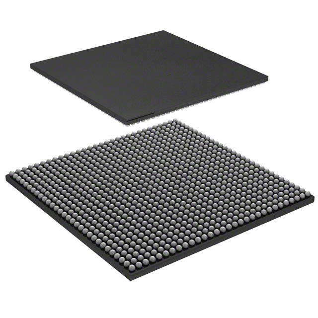
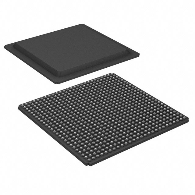
Virtex®-E Field Programmable Gate Array (FPGA) IC 512 294912 15552 680-LBGA Exposed Pad |
|---|---|
| Quantity | 199 Available (as of June 14, 2026) |

| Product Category | Field Programmable Gate Array (FPGA) |
|---|---|
| Manufacturer | AMD |
| Manufacturing Status | Obsolete |
| Manufacturer Standard Lead Time | Contact Us |
| Datasheet |
Specifications & Environmental
| Device Package | 680-FTEBGA (40x40) | Grade | Commercial | Operating Temperature | 0°C – 85°C | ||
|---|---|---|---|---|---|---|---|
| Package / Case | 680-LBGA Exposed Pad | Number of I/O | 512 | Voltage | 1.71 V - 1.89 V | ||
| Mounting Method | Surface Mount | RoHS Compliance | RoHS non-compliant | REACH Compliance | REACH Unaffected | ||
| Moisture Sensitivity Level | 3 (168 Hours) | Number of LABs/CLBs | 3456 | Number of Logic Elements/Cells | 15552 | ||
| Number of Gates | 985882 | ECCN | 3A001A7A | HTS Code | 8542.39.0001 | ||
| Qualification | N/A | Total RAM Bits | 294912 |
Overview of XCV600E-6FG680C – Virtex®-E Field Programmable Gate Array (FPGA) IC 512 294912 15552 680-LBGA Exposed Pad
The XCV600E-6FG680C is a Virtex®-E family FPGA delivered in a 680‑lead LBGA exposed pad package. It provides a mid-density, reprogrammable logic solution with 15,552 logic elements, approximately 0.295 Mbits of embedded memory, and 512 user I/O pins for applications that require substantial logic capacity and flexible I/O connectivity.
Designed for commercial-grade systems, this surface-mount device operates from a core supply range of 1.71 V to 1.89 V and across an operating temperature range of 0 °C to 85 °C, offering a balance of integration, on-chip memory, and I/O density for embedded, communications, and interface-oriented designs.
Key Features
- Logic Capacity — 15,552 logic elements enabling complex digital functions and mid-density system integration.
- Embedded Memory — Approximately 0.295 Mbits (294,912 bits) of on-chip RAM for buffer, FIFO, and state storage directly on the FPGA fabric.
- I/O Density — 512 general-purpose I/O pins to support wide parallel interfaces and multiple high-speed channels.
- Package & Mounting — 680‑lead LBGA exposed pad (supplier package: 680‑FTEBGA, 40×40) in a surface-mount form factor for high-density board designs.
- Power & Temperature — Core supply range 1.71 V to 1.89 V and commercial operating temperature 0 °C to 85 °C for standard embedded and enterprise applications.
- Family-Level Capabilities (from Virtex‑E series) — Includes features such as 1.8 V core operation, high-performance SelectI/O+ standards support, differential signaling options, on-chip clock management (eight DLLs), and SRAM-based in-system reprogrammability as described in the Virtex‑E family specification.
- Standards & Compliance — RoHS compliant, supporting environmental and assembly requirements for lead-free production.
Typical Applications
- Networking & Communications — Implement protocol bridging, packet processing, and interface logic where abundant I/O and embedded RAM are needed for buffering and data path logic.
- Memory Interface Controllers — Act as a programmable interface for high-bandwidth external memories and synchronous SRAM/DDR front-ends using the device’s embedded RAM and configurable logic.
- Data Acquisition & Signal Aggregation — Aggregate and pre-process sensor or instrument data streams using parallel I/O and on-chip memory to stage and route data efficiently.
- In-System Programmable Logic — Reconfigurable control and glue logic for commercial electronic systems requiring field updates or multiple operational modes.
Unique Advantages
- Substantial Mid-Level Logic Density: 15,552 logic elements allow implementation of complex state machines, datapaths, and custom accelerators without external glue logic.
- Generous I/O Count: 512 I/O pins provide flexibility for wide buses, multi-channel interfaces, and mixed-signal partitioning on modern PCBs.
- On-Chip Memory: Nearly 0.295 Mbits of embedded RAM reduces external memory dependency for buffering and small data structures, simplifying BOM and board layout.
- Flexible Packaging: 680‑lead LBGA exposed pad (40×40) supports high-density board placement and thermal conduction for sustained operation in commercial systems.
- Reprogrammability: SRAM-based in-system configuration enables design iterations, firmware-like updates, and field upgrades without hardware changes.
- Regulatory Readiness: RoHS compliance supports lead-free manufacturing processes and environment-driven procurement requirements.
Why Choose XCV600E-6FG680C?
The XCV600E-6FG680C combines a mid-range logic fabric with substantial on-chip memory and a high I/O count in a compact LBGA package, making it well suited for commercial embedded and communications applications that demand programmable logic, flexible interfacing, and in-field reconfiguration. Its 1.8 V family architecture and Virtex‑E series features such as clock management and differential signaling support provide a robust foundation for designs requiring reliable timing and diverse I/O standards.
This part is aimed at teams designing systems where integration, reprogrammability, and I/O bandwidth matter—customers who need a field-updatable FPGA with measurable logic capacity, embedded RAM, and a package optimized for dense PCB layouts will find the XCV600E-6FG680C an effective building block.
Request a quote or submit a purchase inquiry to receive pricing and availability for the XCV600E-6FG680C and to discuss sample and lead-time options.


Date Founded: 1969
Headquarters: Santa Clara, California, USA
Employees: 25,000+
Revenue: $22.68 Billion
Certifications and Memberships: ISO9001:2015, RoHS, REACH


