
XCV600E-6HQ240C
| Part Description |
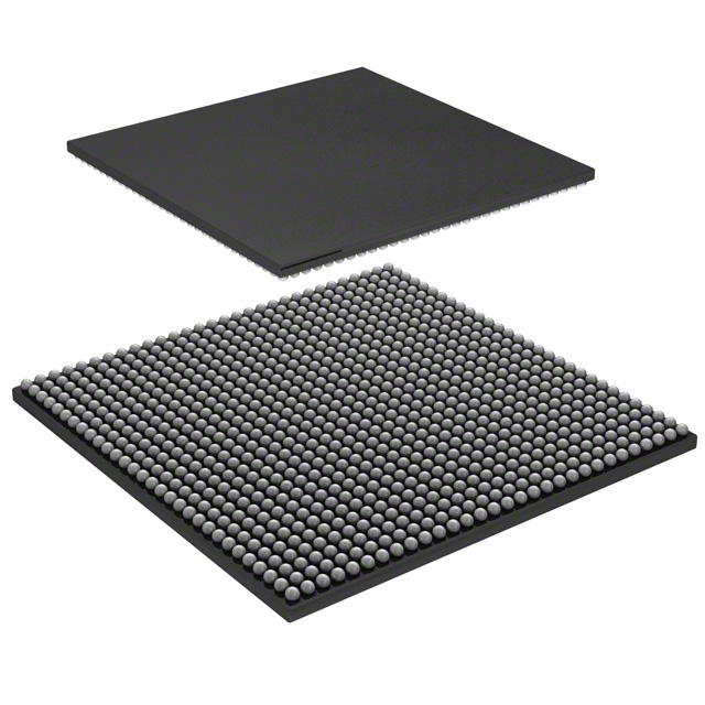
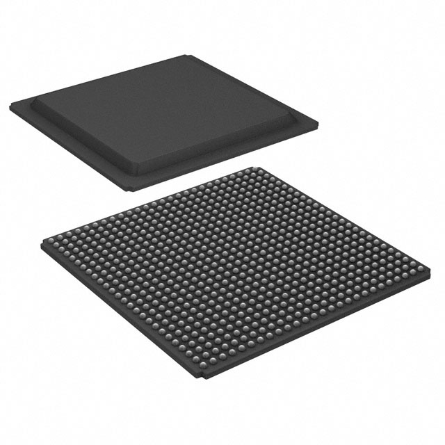
Virtex®-E Field Programmable Gate Array (FPGA) IC 158 294912 15552 240-BFQFP Exposed Pad |
|---|---|
| Quantity | 656 Available (as of June 10, 2026) |

| Product Category | Field Programmable Gate Array (FPGA) |
|---|---|
| Manufacturer | AMD |
| Manufacturing Status | Obsolete |
| Manufacturer Standard Lead Time | Contact Us |
| Datasheet |
Specifications & Environmental
| Device Package | 240-PQFP (32x32) | Grade | Commercial | Operating Temperature | 0°C – 85°C | ||
|---|---|---|---|---|---|---|---|
| Package / Case | 240-BFQFP Exposed Pad | Number of I/O | 158 | Voltage | 1.71 V - 1.89 V | ||
| Mounting Method | Surface Mount | RoHS Compliance | RoHS non-compliant | REACH Compliance | REACH Unaffected | ||
| Moisture Sensitivity Level | 3 (168 Hours) | Number of LABs/CLBs | 3456 | Number of Logic Elements/Cells | 15552 | ||
| Number of Gates | 985882 | ECCN | 3A001A7B | HTS Code | 8542.39.0001 | ||
| Qualification | N/A | Total RAM Bits | 294912 |
Overview of XCV600E-6HQ240C – Virtex®-E Field Programmable Gate Array (FPGA), 240-BFQFP Exposed Pad
The XCV600E-6HQ240C is an AMD Virtex®-E family FPGA offered in a 240-BFQFP exposed-pad surface-mount package. It provides a mid-density FPGA fabric with on-chip memory, high-speed I/O support and reprogrammable SRAM-based configuration suitable for commercial-grade embedded designs.
Built on the Virtex-E 1.8 V architecture, the device targets designs requiring substantial programmable logic (15,552 logic elements), a moderate amount of embedded RAM (294,912 bits), and flexible I/O for high-performance interfaces and memory-centric applications.
Key Features
- Logic Capacity — 15,552 logic elements (reported) delivering programmable fabric for complex combinational and sequential logic implementations.
- Embedded Memory — Approximately 0.295 Mbits of on-chip RAM (294,912 bits) for distributed and block RAM use within designs.
- I/O and Connectivity — 158 I/O pins on the device package to support a variety of external interfaces; Virtex-E family SelectI/O+ technology supports multiple high-performance I/O standards.
- Performance — Series documentation cites internal performance up to 130 MHz (four LUT levels) and support for high-speed differential clock inputs for 300+ MHz clocks.
- Clock Management — Family-level support includes eight fully digital DLLs for clock multiply/divide and DDR duty-cycle synthesis.
- Memory Interface Support — Series-level SelectRAM+ memory hierarchy and architecture designed to interface with high-performance external memories (e.g., ZBT SRAM, DDR SDRAM).
- Supply & Operating Range — Internal supply/logic VCC range listed at 1.71 V to 1.89 V; commercial operating temperature range 0 °C to 85 °C.
- Package & Mounting — 240-BFQFP exposed pad (supplier package listed as 240-PQFP 32×32) and surface-mount mounting type for board-level assembly.
- Regulatory / Environmental — RoHS compliant.
- Reconfigurable SRAM-Based Configuration — SRAM-based in-system configuration enables unlimited re-programmability for iterative development and field updates.
Typical Applications
- High‑performance interface bridging — Implement protocol adaption and buffering between memory and peripheral subsystems using the device's flexible I/O and clocking resources.
- Memory-centric prototyping — Develop and evaluate memory controllers and external-memory interfaces leveraging the on-chip SelectRAM+ architecture and support for ZBT/DDR SDRAM standards at the family level.
- Signal processing and custom logic — Deploy dedicated arithmetic support and abundant registers to implement custom DSP blocks, data aggregation, and pipeline logic.
- PCI/Bus interface designs — Use the Virtex‑E family’s documented PCI compliance (3.3 V, 32/64-bit, 33/66-MHz) at the series level for bus-based system integration.
Unique Advantages
- Balanced logic and memory — 15,552 logic elements paired with ~0.295 Mbits of embedded RAM supports designs that require both programmable logic density and on-chip memory.
- Flexible I/O options — A 158-pin I/O footprint combined with Virtex‑E SelectI/O+ family features enables a wide range of single-ended and differential interface standards.
- Advanced clocking — Eight fully digital DLLs at the family level provide clock multiplication/division and DDR duty-cycle synthesis for complex timing requirements.
- Reprogrammability for iterative development — SRAM-based in-system configuration allows design updates and iterative optimization without hardware replacements.
- Commercial temperature and RoHS compliance — Rated for 0 °C to 85 °C operation and RoHS compliant for standard commercial deployments.
- Surface-mount 240-BFQFP package — Available in a 240-pin BFQFP exposed-pad package (supplier package 240-PQFP 32×32) suitable for surface-mount assembly.
Why Choose XCV600E-6HQ240C?
The XCV600E-6HQ240C positions itself as a reconfigurable mid-density FPGA option within the Virtex‑E family, offering a combination of sizable programmable logic (15,552 logic elements), on-chip memory (294,912 bits), and flexible I/O in a 240-pin exposed-pad PQFP/BFQFP package. It is suited to commercial embedded applications that require in-system reprogrammability, extensive I/O options, and family-level features such as advanced clock management and memory interface support.
For development teams focused on memory interfaces, protocol bridging, or custom processing pipelines, this device delivers a verifiable set of resources and series-proven architectural features to accelerate implementation and iteration while complying with standard commercial operating and environmental requirements.
Request a quote or submit a procurement inquiry to receive pricing and availability information for the XCV600E-6HQ240C.


Date Founded: 1969
Headquarters: Santa Clara, California, USA
Employees: 25,000+
Revenue: $22.68 Billion
Certifications and Memberships: ISO9001:2015, RoHS, REACH


