
XCV600E-6FG676C
| Part Description |
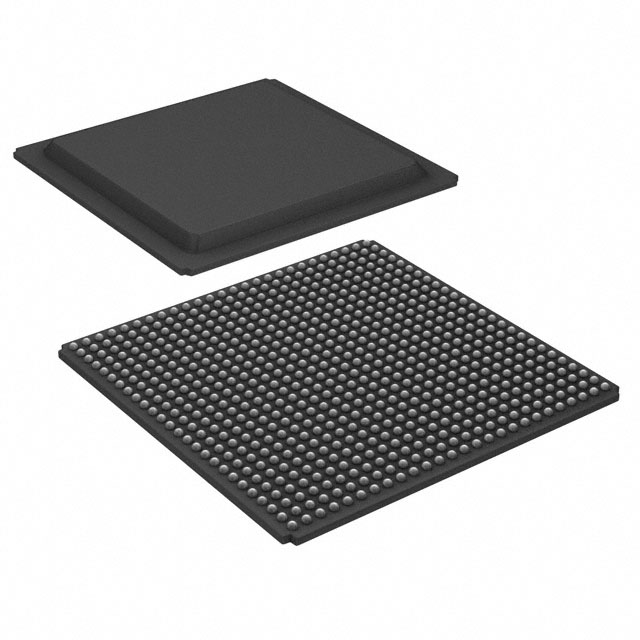
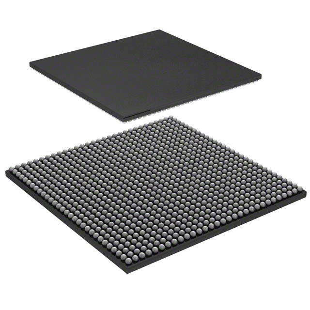
Virtex®-E Field Programmable Gate Array (FPGA) IC 444 294912 15552 676-BGA |
|---|---|
| Quantity | 476 Available (as of June 16, 2026) |
| Product Category | Field Programmable Gate Array (FPGA) |
|---|---|
| Manufacturer | AMD |
| Manufacturing Status | Obsolete |
| Manufacturer Standard Lead Time | Contact Us |
| Datasheet |
Specifications & Environmental
| Device Package | 676-FBGA (27x27) | Grade | Commercial | Operating Temperature | 0°C – 85°C | ||
|---|---|---|---|---|---|---|---|
| Package / Case | 676-BGA | Number of I/O | 444 | Voltage | 1.71 V - 1.89 V | ||
| Mounting Method | Surface Mount | RoHS Compliance | RoHS non-compliant | REACH Compliance | REACH Unaffected | ||
| Moisture Sensitivity Level | 3 (168 Hours) | Number of LABs/CLBs | 3456 | Number of Logic Elements/Cells | 15552 | ||
| Number of Gates | 985882 | ECCN | 3A991D | HTS Code | 8542.39.0001 | ||
| Qualification | N/A | Total RAM Bits | 294912 |
Overview of XCV600E-6FG676C – Virtex®-E Field Programmable Gate Array (FPGA) IC, 676‑BGA, 15,552 logic elements, 444 I/O
The XCV600E-6FG676C is a Virtex®-E family FPGA in a 676‑ball BGA package designed for commercial embedded and interface applications. It integrates 15,552 logic elements, approximately 0.295 Mbits of on-chip RAM (294,912 bits), and 444 user I/O pins to support complex, high-density designs.
Built for 1.8 V core operation (device supply range 1.71 V to 1.89 V) and specified for 0 °C to 85 °C operation, this device combines dense logic, abundant I/O, and programmable memory to accelerate development of custom hardware functions and protocol bridging.
Key Features
- Core & Logic 15,552 logic elements and an equivalent gate count of 985,882 provide substantial programmable logic capacity for medium-to-high complexity designs.
- Embedded Memory Approximately 0.295 Mbits of total on-chip RAM (294,912 bits) for distributed and block RAM allocation to support buffering, FIFOs, and local data storage.
- I/O & Interface Flexibility 444 I/O pins with Virtex‑E SelectI/O+ family capabilities for a wide variety of I/O standards; the Virtex‑E family supports differential signaling standards such as LVDS, BLVDS and LVPECL for high-speed links.
- Clocking & Timing Family-level clock management features include multiple digital DLLs and DDR-capable support to simplify high-speed clocking and data-rate conversion for synchronous interfaces.
- Packaging & Mounting 676‑FBGA (27 × 27) surface-mount package provides a compact footprint for board-level integration while supporting the device’s I/O count and thermal characteristics.
- Power & Operating Range Core supply specified between 1.71 V and 1.89 V; commercial grade operating range from 0 °C to 85 °C. RoHS compliant for regulatory conformance.
- Configuration & Development SRAM-based in-system configuration enables reprogrammability and iterative development; Virtex‑E family devices are supported by established foundation development toolchains noted in the datasheet.
Typical Applications
- High-performance embedded processing — Implement custom accelerators, state machines, and protocol logic where dense logic and on-chip RAM improve latency and throughput.
- High-speed I/O and interface bridging — Use the device’s extensive I/O and differential signaling support to bridge between parallel and serial interfaces or to implement custom PHY logic.
- Memory controller and buffering — On-chip RAM and configurable logic are suitable for implementing memory controllers, FIFOs, and data buffering for external SDRAM/ZBT interfaces.
- Prototyping and in-system reconfiguration — SRAM-based configuration allows rapid iteration and field updates during development and testing cycles.
Unique Advantages
- Substantial programmable capacity: 15,552 logic elements and nearly one million gate-equivalent resources enable implementation of complex digital logic without external ASIC development.
- Versatile I/O options: 444 I/O pins plus family-level SelectI/O+ support for multiple signaling standards reduce the need for external interface components.
- On-chip memory resources: Approximately 0.295 Mbits of embedded RAM supports local buffering and state storage to streamline data-path designs.
- Compact system integration: 676‑FBGA (27×27) package balances I/O density with board-space efficiency for space-constrained systems.
- Commercial-grade and compliant: Device is specified for 0 °C to 85 °C operation and is RoHS compliant to meet common commercial production requirements.
Why Choose XCV600E-6FG676C?
The XCV600E-6FG676C offers a balanced combination of logic density, embedded memory, and flexible I/O in a commercially rated package. It is well suited for development teams needing reprogrammable hardware to accelerate system functions, implement custom interfaces, or prototype complex digital designs without committing to fixed silicon.
With support for family-level clocking and differential signaling capabilities, this Virtex‑E device delivers the integration and reconfigurability necessary for mid-to-high complexity embedded and interface applications, while meeting common commercial temperature and environmental requirements.
Request a quote or submit a purchase inquiry to receive pricing and availability information for XCV600E-6FG676C.


Date Founded: 1969
Headquarters: Santa Clara, California, USA
Employees: 25,000+
Revenue: $22.68 Billion
Certifications and Memberships: ISO9001:2015, RoHS, REACH


