
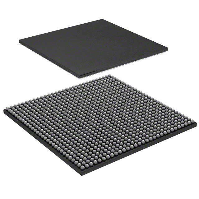
XCV600E-6FG676I
| Part Description |
Virtex®-E Field Programmable Gate Array (FPGA) IC 444 294912 15552 676-BGA |
|---|---|
| Quantity | 1,168 Available (as of June 18, 2026) |

| Product Category | Field Programmable Gate Array (FPGA) |
|---|---|
| Manufacturer | AMD |
| Manufacturing Status | Obsolete |
| Manufacturer Standard Lead Time | Contact Us |
| Datasheet |
Specifications & Environmental
| Device Package | 676-FBGA (27x27) | Grade | Industrial | Operating Temperature | -40°C – 100°C | ||
|---|---|---|---|---|---|---|---|
| Package / Case | 676-BGA | Number of I/O | 444 | Voltage | 1.71 V - 1.89 V | ||
| Mounting Method | Surface Mount | RoHS Compliance | RoHS non-compliant | REACH Compliance | REACH Unaffected | ||
| Moisture Sensitivity Level | 3 (168 Hours) | Number of LABs/CLBs | 3456 | Number of Logic Elements/Cells | 15552 | ||
| Number of Gates | 985882 | ECCN | 3A991D | HTS Code | 8542.39.0001 | ||
| Qualification | N/A | Total RAM Bits | 294912 |
Overview of XCV600E-6FG676I – Virtex®-E Field Programmable Gate Array (FPGA) IC, 676-BGA
The XCV600E-6FG676I is a Virtex®-E family FPGA provided in a 676-ball FBGA (27×27) package, optimized for industrial applications. This SRAM-based, reprogrammable device combines a high logic element count with substantial I/O and embedded memory to support complex digital designs.
Key capabilities exposed by the device include a large number of logic elements, high I/O density, on-chip RAM, and support for advanced I/O signaling and clock management as documented for the Virtex‑E family.
Key Features
- Programmable Core Approximately 15,552 logic elements provide the configurable fabric required for complex control, signal processing, and glue-logic implementations.
- Embedded Memory Approximately 0.29 Mbits (294,912 bits) of on-chip RAM to support buffering, FIFOs, and small internal memory structures.
- I/O Density and Bandwidth 444 user I/O pins offer high I/O concurrency for parallel interfaces and wide buses.
- Advanced I/O and Differential Signaling Family-level Virtex‑E technology supports SelectI/O+ interface options and differential standards such as LVDS, BLVDS, and LVPECL for high-speed serial and source-synchronous links.
- Clock Management The Virtex‑E family provides multiple fully digital Delay-Locked Loops (DLLs) for clock multiplication/division and duty-cycle control to support complex timing requirements.
- Power and Interface Supply Core supply range is specified from 1.71 V to 1.89 V, matching the 1.8 V Virtex‑E core specification.
- Industrial Temperature Grade Qualified for operation from −40 °C to 100 °C for reliable performance in industrial environments.
- Package and Mounting Supplied in a 676-FBGA (27×27) surface-mount package for compact board-level integration.
- Manufacturing and Test The device is factory tested and provided as an SRAM-based, in-system reprogrammable FPGA for iterative development and deployment.
Typical Applications
- Industrial Control and Automation Use the device’s industrial temperature rating and high I/O count for motor control, PLC I/O expansion, and real-time control logic.
- High-Speed Interfaces and Networking Leverage SelectI/O+ and differential signaling support for source-synchronous interfaces, protocol bridging, and custom packet processing.
- Memory and Bus Interface Bridging Embedded RAM and programmable logic enable custom buffering, arbitration, and interface adaptation between disparate memory and peripheral standards.
- Prototyping and In-System Reconfiguration SRAM-based reprogrammability supports iterative development, functional updates, and design validation without changing hardware.
Unique Advantages
- High Logic Capacity: Approximately 15,552 logic elements provide the resources needed for medium-complexity FPGA designs without external glue logic.
- Substantial I/O Count: 444 I/Os enable wide parallel buses and multiple concurrent interface channels on a single device.
- On-Chip Memory: Approximately 0.29 Mbits of embedded RAM reduces dependence on external memory for small buffering and state storage.
- Industrial Reliability: Rated for −40 °C to 100 °C operation to meet environmental demands of factory and fielded systems.
- Flexible Clocking: Multiple DLLs and family clock-management features simplify clock domain control and DDR timing requirements.
- Compact, Surface-Mount Package: 676-FBGA (27×27) packaging offers a dense solution for space-constrained PCBs.
Why Choose XCV600E-6FG676I?
The XCV600E-6FG676I positions itself as a versatile Virtex‑E family FPGA for engineers who need a balanced combination of logic capacity, I/O density, and embedded memory within an industrial temperature envelope. Its programmable core and on-chip resources make it suitable for designs requiring in-system reconfiguration and reliable operation across extended temperature ranges.
For teams implementing mid-range FPGA designs—such as industrial controllers, interface bridges, and high-speed I/O modules—this device offers a traceable specification set, compact package, and the reprogrammability advantages of SRAM-based FPGAs.
Request a quote for the XCV600E-6FG676I to check current availability and pricing for your next design.


Date Founded: 1969
Headquarters: Santa Clara, California, USA
Employees: 25,000+
Revenue: $22.68 Billion
Certifications and Memberships: ISO9001:2015, RoHS, REACH


