
XCV600E-6HQ240I
| Part Description |
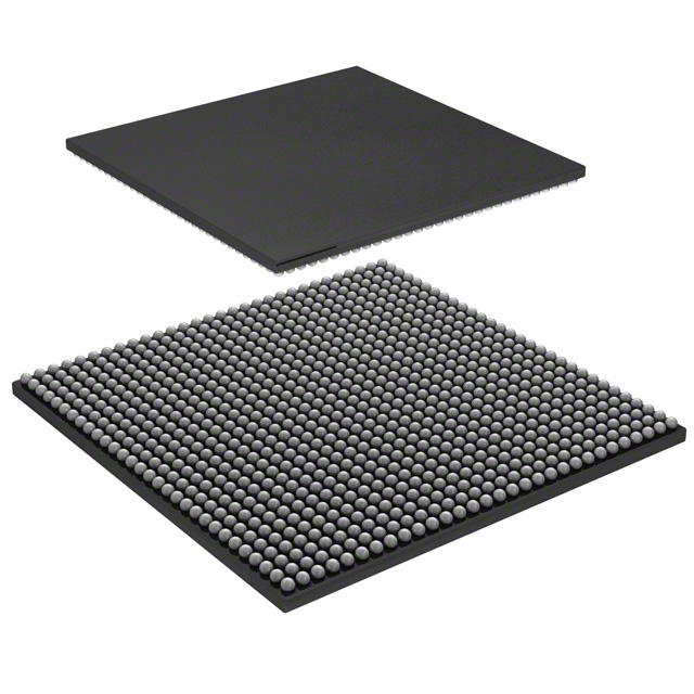
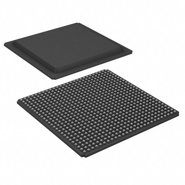
Virtex®-E Field Programmable Gate Array (FPGA) IC 158 294912 15552 240-BFQFP Exposed Pad |
|---|---|
| Quantity | 96 Available (as of June 10, 2026) |

| Product Category | Field Programmable Gate Array (FPGA) |
|---|---|
| Manufacturer | AMD |
| Manufacturing Status | Obsolete |
| Manufacturer Standard Lead Time | Contact Us |
| Datasheet |
Specifications & Environmental
| Device Package | 240-PQFP (32x32) | Grade | Industrial | Operating Temperature | -40°C – 100°C | ||
|---|---|---|---|---|---|---|---|
| Package / Case | 240-BFQFP Exposed Pad | Number of I/O | 158 | Voltage | 1.71 V - 1.89 V | ||
| Mounting Method | Surface Mount | RoHS Compliance | RoHS non-compliant | REACH Compliance | REACH Unaffected | ||
| Moisture Sensitivity Level | 3 (168 Hours) | Number of LABs/CLBs | 3456 | Number of Logic Elements/Cells | 15552 | ||
| Number of Gates | 985882 | ECCN | 3A001A7B | HTS Code | 8542.39.0001 | ||
| Qualification | N/A | Total RAM Bits | 294912 |
Overview of XCV600E-6HQ240I – Virtex®-E FPGA, 240-BFQFP Exposed Pad
The XCV600E-6HQ240I is an AMD Virtex®-E Field Programmable Gate Array (FPGA) in a 240‑pin BFQFP exposed‑pad package for surface‑mount assembly. It delivers a programmable logic fabric with 15,552 logic elements, approximately 0.295 Mbits of embedded memory, and 158 general‑purpose I/Os for systems that require mid‑range gate density and flexible I/O integration.
Designed for industrial applications, this device supports a 1.71 V to 1.89 V core supply range, operates from –40 °C to 100 °C, and is RoHS compliant—providing a balance of performance, integration, and environmental compliance for embedded and communications designs.
Key Features
- Logic Capacity Approximately 15,552 logic elements (reported as 15552 logic elements) corresponding to 985,882 gates for implementing medium‑complexity digital systems.
- Embedded Memory Approximately 0.295 Mbits of on‑chip RAM (294,912 total RAM bits) to support data buffering, FIFOs, and distributed storage.
- I/O Count & Flexibility 158 I/Os delivered in a 240‑pin BFQFP exposed‑pad package; family datasheet highlights broad differential and single‑ended I/O standards for high‑speed interfacing.
- Clock & Timing Family documentation describes advanced clock management with multiple DLLs for synthesized clocks and DDR support—beneficial for timing‑critical designs.
- Power & Supply Core supply range 1.71 V to 1.89 V, enabling operation at 1.8 V nominal VCCINT as indicated for the Virtex‑E family.
- Package & Thermal 240‑BFQFP with exposed pad, surface‑mount mounting, and an industrial operating temperature range of –40 °C to 100 °C to support robust thermal management and board‑level assembly.
- Configuration & Development SRAM‑based in‑system configuration provides unlimited re‑programmability; family resources are supported by established development tool flows.
- Regulatory & Quality RoHS compliant and 100% factory tested per family production specification.
Typical Applications
- Communications Equipment Protocol processing, interface bridging, and mid‑rate data aggregation where programmable logic and flexible I/O standards are required.
- Memory Interface & Controllers High‑performance interfaces to external memories and buffering applications that leverage the device’s embedded RAM and clock management features.
- Industrial Control & Automation Logic consolidation, sensor interfacing, and custom control functions benefiting from the industrial temperature rating and re‑programmability.
- Prototyping & Reconfigurable Systems SRAM‑based in‑system reprogramming enables iterative development and field upgrades for evolving system requirements.
Unique Advantages
- Substantial Logic Resources: The 15,552 logic elements and ~985,882‑gate equivalent provide ample capacity for mid‑complexity FPGA designs without immediate migration to larger devices.
- Integrated On‑Chip Memory: Approximately 0.295 Mbits of embedded RAM reduces external memory dependence for many buffering and register file needs, simplifying BOM and board routing.
- Flexible I/O in a Compact Package: 158 I/Os in a 240‑pin exposed‑pad BFQFP support varied interface requirements while retaining a compact footprint for dense assemblies.
- Industrial Temperature Range: Rated from –40 °C to 100 °C to support deployment in harsher environments and extended operating conditions.
- SRAM‑Based Reprogrammability: In‑system configuration enables field updates and design iteration without hardware changes.
- RoHS Compliant & Factory Tested: Conforms to environmental requirements and is 100% factory tested at the family level for production reliability.
Why Choose XCV600E-6HQ240I?
The XCV600E-6HQ240I offers a balanced combination of programmable logic capacity, embedded memory, and flexible I/O in a surface‑mount 240‑BFQFP exposed‑pad package. Its industrial temperature rating and RoHS compliance make it a practical choice for embedded and communications applications that require reliable, reconfigurable logic with moderate gate density.
Backed by the Virtex‑E family’s documented features and development ecosystem, this device is well suited for engineers seeking a reprogrammable platform that supports high‑performance I/O, on‑chip memory, and robust clock management while maintaining a compact board footprint.
Request a quote or submit a pricing and availability inquiry for XCV600E-6HQ240I to get started with procurement and lead‑time details.


Date Founded: 1969
Headquarters: Santa Clara, California, USA
Employees: 25,000+
Revenue: $22.68 Billion
Certifications and Memberships: ISO9001:2015, RoHS, REACH


